3.1 Introduction
This chapter presents a concise treatment of S-parameters, meant primarily as an introduction to the more general formalism of large-signal approaches of the next chapter. The concepts of time invariance and spectral maps are introduced at this stage to enable an easier generalization in the ensuing chapter. The interpretations of S-parameters as calibrated measurements, intrinsic properties of the device-under-test (DUT), intellectual property (IP)-secure component behavioral models, and composition rules for linear system design are presented. The cascade of two linear S-parameter components is considered as an example to be generalized to the nonlinear case later. The calculation of S-parameters for a transistor from a simple nonlinear device model is used as an example to introduce the concepts of (static) operating point and small-signal conditions, both of which must be generalized for the large-signal treatment.
3.2 S-parameters
Since the 1950s, S-parameters, or scattering parameters, have been among the most important of all the foundations of microwave theory and techniques.
S-parameters are easy to measure at high frequencies with a vector network analyzer (VNA). Well-calibrated S-parameter measurements represent properties of the DUT, independent of the VNA system used to characterize it. Calibration procedures [2] remove systematic measurement errors and enable a separation of the overall values into numbers attributable to the device, independent of the measurement system used to characterize it. In this context, we call such properties intrinsic.1 These DUT properties (gain, loss, reflection coefficient, etc.) are familiar, intuitive, and important [3]. Another key property of S-parameters is that the S-parameters of a composite system are completely determined from knowledge of the S-parameters of the constituent components and their connectivity. S-parameters provide the complete specification of how a linear component responds to an arbitrary signal. Therefore, simulations of linear systems that are designed by cascading S-parameter blocks are predictable with certainty. S-parameters define a complete behavioral description of the linear component at the external terminals, independent of the detailed physics or specifics of the realization of the component. S-parameters can be shared between component vendors and system integrators freely, without the possibility that the component implementation can be reverse engineered, protecting IP and promoting sharing and reuse. Indeed, one may ask the question, “are S-parameters measurements, or do they constitute a model?” The answer is really “both.” They are numbers that can be measured accurately at RF and microwave frequencies, and these numbers are the coefficients of a behavioral model that expresses the scattered waves as linear contributions of the incident waves.
S-parameters need not come only from measurements. They can be calculated from physics by solving Maxwell’s equations, by linearizing the semiconductor equations, or computed from matrix analysis of linear equivalent circuits. In this way, the many benefits of S-parameters can be realized starting from a more detailed representation of the component from first principles or from a complicated linear circuit model.
Graphical methods based around the Smith Chart were invented to visualize and interpret S-parameters and graphical design methodologies soon followed for circuit design [3], [4]. These days, electronic design automation (EDA) tools provide simulation components – S-parameter blocks – and design capabilities using the familiar S-parameter analysis mode.
One of the great utilities of S-parameters is the interoperability among the measurement, modeling, and design capabilities they provide. One can characterize the component with measured S-parameters, use them as a high-fidelity behavioral model of the component with complete IP protection, and design systems with them in the EDA environment.
3.3 Wave Variables
The term scattering refers to the relationship between incident and scattered (reflected and transmitted) travelling waves.
By convention, in this text the circuit behavior is described using generalized power waves [5], although there are alternative wave-definitions used in the industry.
The wave variables, AA and BB, corresponding to a specific port of a network, are defined as simple linear combinations of the voltage and current, VV and II, at the same port, according to Figure 3.1 and equations (3.1).
 (3.1)
(3.1)The reference impedance for the port, Z0Z0, is, in general, a complex value. For the purpose of simplifying the concepts presented, the reference impedance is restricted to real values in this text.
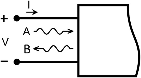
Figure 3.1 Wave definitions.
The currents and voltages can be recovered from the wave variables, according to equations (3.2).
 (3.2)
(3.2)Here AA and BB represent the incident, scattered waves VV and II are the port voltage and current, respectively, and Z0Z0 is the reference impedance for the port. Z0Z0 can be different for each port, but we do not consider that further here. A typical value of Z0Z0 is 50 Ω by convention, but other choices may be more practical for some applications. A value for Z0Z0 closer to 1 Ω is more appropriate for S-parameter measurements of power transistors, for example, given that power transistors typically have very small output impedances.
The variables in equations (3.1) and (3.2) are complex numbers representing the RMS-phasor description of sinusoidal signals in the frequency domain. Later we will generalize to the envelope domain by letting these complex numbers vary in time.
A, B, V,A,B,V, and II can be considered RMS-vectors, the components of which indicate the values associated with sinusoidal signals at particular ports labeled by positive integers. Thus AjAj is the incident wave RMS-phasor at port j and IkIk is the current RMS-phasor at port k. For now, Z0Z0 is taken to be a fixed real constant, in particular, 50 Ω.
A graphical representation of the wave description is given in Figure 3.2 for the case of a system described by a two-port device. For definiteness, we assume a port description with a common reference pin, as indicated in the figure.
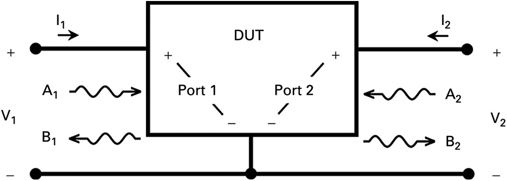
Figure 3.2 Incident and scattered waves of a two-port device. All ports should be referenced to the same pin for modeling purposes.
To retrieve the time-dependent sinusoidal voltage signal at the ith port, the complex value of the phasor and also the angular frequency, ωω, to which the phasor corresponds, must be known. The voltage is then given by (3.3), and, similarly, for the other variables, where Vipk are peak values.
 (3.3)
(3.3)It is convenient to keep track of the frequency associated with a particular set of phasors by rewriting (3.1) according to (3.4), and (3.2) according to (3.5), where the port indexing notation is made explicit.
 (3.4)
(3.4) (3.5)
(3.5)For each angular frequency, ωω, Eq. (3.4) is a set of two equations defined at each port.
The assumption behind the S-parameter formalism is that the system being described is linear and therefore there must be a linear relationship, implying superposition holds, between the phasor representation of incident and scattered waves. This is expressed in (3.6) for an N-port network:
 (3.6)
(3.6)The set of complex coefficients, Sij(ω)Sijω, in (3.6) define the S-parameter matrix, or simply, the S-parameters, at that frequency. Equation (3.6), for the fixed set of complex S-parameters, determines the output phasors for any set of input phasors. The summation is over all port indices, so that incident waves at each port, j, contribute in general to the overall scattered wave at each output port, i. For now we consider all frequencies to be positive (ω>0ω>0). Note that contributions to a scattered wave at frequency ωω come only from incident waves at the same frequency. This is not the case for the more general X-parameters, where a stimulus at one frequency can lead to scattered waves at different frequencies.
For definiteness and later reference, the S-parameter equations for a linear two-port are written explicitly in (3.7).
 (3.7)
(3.7)The set of equations (3.6) represent a model of the network under study. For the purpose of creating a model for the network, all ports should be referenced to the same pin, as shown in Figure 3.2.
Such connectivity is the natural option for the measurement and modeling process of a 3-pin network (like a transistor) but it has to be extended in the general case of an arbitrary network and it is necessary for all networks, linear and/or nonlinear. This connectivity convention is considered by default (unless otherwise specified) for the remaining of this text.
Using the topological connection in Figure 3.2, the set of equations (3.6) represent a complete model of the network under test.
From (3.6) we note a stimulus (incident wave) at a particular port j will produce a response (scattered wave) at all ports, including the port at which the stimulus is applied.
3.4 Geometrical Interpretation of S-parameters
For linear two-port components described by (3.7), the scattering of A2 at port 2 is given simply by S22 A2, where S22 is just a fixed complex number. This means we can write for ΔB2 = B2 − S21A1ΔB2=B2−S21A1
For fixed |A2|A2, S22A2 = S22|A2|ejϕ(A2)S22A2=S22A2ejϕA2, so by varying ϕ(A2)ϕA2 from 0 to 2π2π radians, equation (3.8) traces out a circle with radius |A2|S22A2. This is shown in Figure 3.3.

Figure 3.3 Locus of points produced from S-parameter equation (3.8) evaluated for all phases of A2A2. The radius of the circle is |S22 A2|S22A2.
This fact is trivial in the case of S-parameters. We will see in the next chapter that the scattering of even a small-signal A2 has a different (non-circular) geometry when a nonlinear component is driven with a large A1 signal.
3.5 Nonlinear Dependence on Frequency
Equation (3.6) shows that the scattered waves are linear functions of the complex amplitudes (the phasors) of the incident waves, with the S-parameters being the coefficients of the linear relationship. These coefficients, however, have a frequency dependence that is usually not linear. That is, we generally have Sij(λω)≠λSij(ω)Sijλω≠λSijω for λλ a positive real number. For example, an ideal band-pass filter response is linear in the incident wave phasor, but the filter response is a nonlinear function of the frequency of the incident wave. This is shown in Figure 3.4.

Figure 3.4 A linear network has a linear behavior versus input power level, but the dependence on frequency is usually not linear.
3.6 S-parameter Measurement
3.6.1 Conventional Identification
By setting all incident waves to zero in (3.6), except for AjAj, one can deduce the simple relationship between a given S-parameter (S-parameter matrix element) and a particular ratio of scattered to incident waves according to (3.9). Sometimes (3.9) is taken as the definition of the S-parameters for a linear system, instead of our starting point (3.6). However, since we will show an alternative identification method for S-parameters in Section 3.6.2, we prefer to interpret (3.9) as a simple consequence of the more fundamental linearity principle, (3.6).
 (3.9)
(3.9)Equation (3.9) corresponds to a simple graphical representation shown in Figure 3.5 for the simple case of a two-port component. In Figure 3.5 a, the stimulus is a wave incident at port 1. The fact that A2A2 is not present (A2 = 0A2=0) is interpreted to mean that the B2B2 wave scattered and travelling away from port 2 is not reflected back into the device at port 2. Under this condition, the device is said to be perfectly matched at port 2. Two of the four complex S-parameters, specifically S11 and S21S11andS21, can be identified using (3.9) for this case of exciting the device with only A1A1. Figure 3.5b shows the case where the device is stimulated with a signal, A2A2, at port 2, and assumed to be perfectly matched at port 1 (A1 = 0A1=0). The remaining S-parameters, S12 and S22S12andS22, can be identified from this ideal experiment.

Figure 3.5 S-parameter experiment design.
3.6.2 Alternative Identification
The S-parameters may also be determined by a direct solution of (3.6) from multiple measurements of the BiBi in response to excitations in which the AjAj have multiple (relative) phases.
The S-parameters at a particular frequency may also be determined by a direct solution of (3.6) by measuring the scattered waves in response to known excitations by incident waves at multiple ports simultaneously. Exciting the device by multiple signals can be useful, even for linear components, because, for example, there is no need to switch a signal from one port to the others or to perfectly match the other ports as required in the ideal conventional case. For the nonlinear case of the next chapter, we will have to use simultaneous excitations. Let’s use a simple two-port [N = 2 in (3.6)] example to illustrate the concept.
In this case there are four complex S-parameters to be determined from the measured responses at both ports, BiBi, to the known excitations simultaneously at each port, AjAj. Therefore, we need at least two sets of independent excitations, Ajn , and the corresponding responses, Bin
 , where the superscript, n, labels the experiment number. In matrix notation we have
 (3.10)
Equation (3.10) is a set of four complex equations for the four unknown S-parameters, SijSij given the four measured Bin responses to the four stimuli Ajn
 . The formal solution is given in matrix notation in (3.11).
More generally, for more robust results, there can be more data [columns for the first and third matrices in (3.10)] than unknowns and the formal solution is given in terms of pseudo-inverses according to (3.12). According to the discussion in Chapter 1, this provides the best S-matrix in the least squares sense:
3.6.3 S-parameter Measurement for Nonlinear Components
It is important to note that the ratio on the right-hand side of (3.9) can be computed from independent measurements of incident and scattered waves for actual components corresponding to any nonzero value for the incident wave, AjAj. The value of this ratio, however, will generally vary with the magnitude of the incident wave. Therefore, the identification of this ratio with the S-parameters of the component is valid for any particular value of incident AjAj only if the component behaves linearly, namely according to (3.6). In other words, the values of the incident waves, AjAj, need to be in the linear region of operation for this identification to be valid. For nonlinear components, such as transistors biased at a fixed voltage, the scattered waves don’t continue indefinitely to increase as the incident waves get larger in magnitude (this is compression). Therefore, different values of (3.9) result from different values of incident waves. A better definition of S-parameters for a nonlinear component is a modification of (3.9) given by (3.13). That is, for a general component, biased at a constant DC-stimulus, the S-parameters are related to ratios of output responses to input stimuli in the limit of small input signals. This emphasizes that S-parameters properly apply to nonlinear components only in the small-signal limit.
 (3.13)
3.7 S-parameters as a Spectral Map
If there are multiple frequencies present in the input spectrum, one can represent the output spectrum in terms of a matrix giving the contributions to each output frequency from each input frequency.
An example in the case of three input frequencies is given by Eq. (3.14). Here we assume a single port, for simplicity, and therefore drop the port indices. It is clear from (3.14) that S-parameters are a diagonal map in frequency space. This means each output frequency contains contributions only from inputs at that same frequency. Or, in other words, each input frequency never contributes to outputs at any different frequency.
 (3.14)
A graphical representation is given in Figure 3.6 for the case of forward transmission through a two-port network with matched terminations at both ports.

Figure 3.6 Linear spectral map through S-parameters matrix.
The interpretation of Figure 3.6, mathematically represented by (3.14), is that S-parameters define a particularly simple linear spectral map relating incident to scattered waves. S-parameters are diagonal in the frequency part of the map, namely they predict a response only at the particular frequencies of the corresponding input stimuli. It will be demonstrated in later chapters that the large-signal approaches provide for richer behavior.
For signals with a continuous spectrum, the diagonal nature of the S-parameter spectral map can be written as
 (3.15)
Performing the integration over input frequencies in (3.15) results in Equation (3.6), the form usually given for S-parameters.
3.8 Superposition
Any linear theory, like S-parameters, enables the general response to an arbitrary input signal to be computed by superposition of the responses to unit stimuli (see the discussion of the impulse response in Chapter 1, Section 2). Superposition enables great simplifications in analysis and measurement. Superposition is the reason S-parameters can be measured by independent experiments with one sinusoidal stimulus at a time, one stimulus per port per frequency using Eq. (3.9). The general response to any set of input signals can be obtained by superposition using Eq. (3.6).
An example of superposition is shown in Figure 3.7, with all signals represented both in time and frequency domains.

Figure 3.7 Superposition example.
This example uses two signals, each containing two frequency components, as stimuli incident at each port, independently, with the other port perfectly matched. The example shows that the response to a linear combination of the stimuli is the same linear combination of the individual responses.
As always, the caveat is that the component actually behaves linearly over the range of signal levels used to stimulate the device. There is no a priori way to know whether a component will behave linearly without precise knowledge about its composition or physical or measured characteristics.
3.9 Time Invariance of Components Described by S-parameters
A DUT description in terms of S-parameters defined by (3.6) naturally embodies an important principle known as time invariance. Time invariance states that if y(t)yt is the DUT response to an excitation, x(t)xt, then the DUT response to the time-shifted excitation, x(t − τ)xt−τ, must be y(t − τ)yt−τ. This must be true for all time-shifts, ττ. That is, if the input is shifted in time, the output is shifted by the corresponding amount but is otherwise identical with the DUT response to the nonshifted input. This is stated mathematically in (3.16), where O is the operator taking input to output:
Time invariance is a property of common linear and nonlinear components, such as passive inductors, capacitors, resistors, and diodes, and active devices such as transistors. Examples of components not time-invariant (in the usual sense) are oscillators and other autonomous systems.
The proof follows from elementary properties of the Fourier Transform, where a phase shift by ejωτejωτ in the frequency domain corresponds to a time shift of ττ in the time domain. The time-domain waves incident at the ports (the stimuli) are aj(t)ajt and their Fourier transforms are Ajpkω , as in equation (3.17). In (3.17), the symbol F
 denotes the Fourier transform. The superscript, (pk), in (3.17) refers to peak value (as opposed to the power-wave value).
 (3.17)
The time-domain waves scattered from the ports (the response) are bi(t)bit and their Fourier transforms are Bipkω , as in equation (3.18).
 (3.18)
If all stimuli are delayed with the same time-delay, ττ, the response becomes
 (3.19)
Equation (3.19) proves that S-parameters are automatically consistent with the principle of time invariance. Therefore, any set of S-parameters describes a time-invariant system.
Unlike the case for S-parameters, a more general (e.g., nonlinear) relationship between incident A waves and scattered B waves is not automatically consistent with the property (3.16) of time invariance. This will be demonstrated in Chapter 4. Therefore, in order to have a consistent representation of a nonlinear time-invariant DUT, the time-invariance property must be manifestly incorporated into the mathematical formulation of the behavioral model relating input to output waves. A representation of a time-invariant DUT by equations not consistent with (3.16) means the model is fundamentally wrong and can yield very inaccurate results for some signals, even if the model “fitting” (or identification) appears good at time t.
3.10 Cascadability
Another key property of S-parameters is that the response of a linear circuit or system can be computed with perfect certainty knowing only the S-parameters of the constituent components and their interconnections. The overall S-parameters of the composite design can be calculated by using (3.6) in conjunction with Kirchhoff’s Voltage Law (KVL) and Kirchhoff’s Current Law (KCL) applied at the internal nodes created by connections between two or more components.
This is illustrated for a cascade of two-ports in Figure 3.8a. Each component is characterized by its own S-parameter matrix, S(1)S1 and S(2)S2, respectively. The output port (subscript number 2) of the first component is connected to the input port (subscript number 1) of the second component, creating an internal node.

Figure 3.8 The cascade of 2 two-ports.
It is a straightforward exercise to write the two equations that follow from applying KVL and KCL at the internal node. These are given by equations (3.20) and (3.21)
 (3.20)
 (3.21)
Each two-port relates two input and two output variables. When cascaded, equations (3.20) and (3.21) can be used to compute the overall S-parameter matrix of the composite. The result is given in equation (3.22).
 (3.22)
A network characterized by the ScompositeScomposite is equivalent to the cascade of the two DUTs, yielding the same response under the same stimuli. This is shown in Figure 3.8b.
3.11 DC Operating Point: Nonlinear Dependence on Bias
For devices such as diodes and transistors, the S-parameter values depend very strongly on the DC bias conditions defining the component operating conditions. For example, a FET transistor biased in the saturation region of operation will have S-parameters appropriate for an active amplifier (where |S21|>>1>>|S12|S21≫1≫S12) whereas when biased “off” (say VDS = 0VDS=0) the S-parameters will represent the characteristics of a passive switch (S21 = S12S21=S12 with |Sij| < 1Sij<1).
3.12 S-parameters of a Nonlinear Device
It is possible to derive the S-parameters of a transistor starting from a simple nonlinear model of the intrinsic device. The process illustrates the concept of linearizing a nonlinear mapping about an operating point. This concept, suitably generalized, is a foundation for X-parameters and similar approaches in the next chapter.
The equivalent circuit of a simple, unilateral FET model is shown in Figure 3.9. More complete model topologies and equations are discussed in Chapter 5 and [7].

A current source, iDSiDS, represents the nonlinear bias-dependent channel current from drain to source, and a simple nonlinear two-terminal capacitor, qGSqGS, represents the nonlinear charge storage between gate and source terminals.
The large-signal model equations corresponding to this equivalent circuit are given by (3.23) and (3.24), where the stimulus applied to the device is the set of port voltages, vGSvGS and vDSvDS, and the device response is the set of port currents, iGSiGS and iDSiDS:
 (3.23)
Equations (3.23) and (3.24) are evaluated for time-varying voltages assumed to have a fixed DC component and a small sinusoidal component at a single RF or microwave angular frequency, ω = 2πfω=2πf. Port 1 is associated with the gate and port 2 with the drain terminals, referenced to the source.
For a stimulus comprising a combination of DC and one sinusoidal signal per port, the voltages are formally expressed as shown in (3.25). The symbol δδ is used to emphasize that such terms are considered sufficiently small that simple perturbation theory can be applied to simplify the ensuing analysis.
 (3.25)
Expressions in (3.26) and (3.27) are obtained by substituting (3.25) for i = 1,2, into (3.23) and (3.24), and evaluating the result to first order in the real quantities δViδVi.
 (3.26)
 (3.27)
Here the following definitions of the linearized equivalent circuit elements have been used:
 (3.28)
By equating the 0th order terms in δViδVi, the operating point conditions are obtained:
 (3.29)
Equating the first order terms in δViδVi leads to
 (3.30)
Equation (3.30) is expressed in the frequency domain by defining complex phasors δI(ω)δIω and δV(ω)δVω according to (3.31):
 (3.31)
Equations (3.30) can be rewritten for the complex phasors in matrix notation as
 (3.32)
where
 (3.33)
Equation (3.33) defines the (common source) admittance matrix of the model. The matrix elements are evidently functions of the DC operating point (bias conditions) of the transistor and also the (angular) frequency of the excitation.
Since the phasors representing the port voltage and currents in (3.32) can be reexpressed as linear combinations of incident and scattered waves using (3.5), it is possible to derive the expression for the S-parameters in terms of the Y-parameters (admittance matrix elements). This results in the well-known conversion formula (3.34) [3]:2
Here II is the two-by-two unit matrix, Z0Z0 is the reference impedance used in the wave definitions in (3.4), YY is the two-port admittance matrix, and SS is the corresponding S-parameter matrix. Substituting (3.33) into (3.34) results in an explicit expression, (3.35), for the S-parameters corresponding to this simple model in terms of the linear equivalent circuit element values given in (3.28):
 (3.35)
In summary, the S-parameters of a nonlinear component can be derived or computed by linearizing the full nonlinear characteristics of the circuit equations around a static (DC) operating point defined by the voltage or current bias conditions. The S-parameters define a linear relationship between the incident and scattered waves at a fixed DC operating point of the device and fixed frequency for the incident waves. The S-parameters are an accurate description of how the device responds to signals, provided the signal amplitude is sufficiently small that the DC operating point is not significantly affected by the signal. This will almost always be the case for signals of sufficiently small amplitude.
3.13 Additional Benefits of S-parameters
3.13.1 Applicable to Distributed Components at High Frequencies
S-parameters can accommodate an arbitrary frequency-dependence in the linear spectral mapping. S-parameters therefore apply when describing distributed components for which lumped approximations are not very accurate or efficient. This is especially true for high-frequency microwave components when the typical wavelengths of the stimulus approach and become smaller than the physical size of the component. The simplest example is the case of linear transmission lines. Another common example is the case of an active device, for which measured S-parameters of a transistor can be much more accurate than those computable from the linearized lumped nonlinear model. This is especially true as the frequency approaches and exceeds the device cutoff frequency, fTfT, beyond which a distributed representation is generally required.
3.13.2 S-parameters Are Easy to Measure at High Frequencies
S-parameters contain no more information than the familiar Y and Z-parameters of elementary linear circuit theory, yet they have great practical advantages. S-parameters are much easier to measure at high frequencies. Y and Z-parameters require short and open circuit boundary conditions, respectively, on the components for a direct measurement. Short and open circuit conditions are hard to achieve at microwave frequencies, and so are impractical. Moreover, such conditions presented to a power transistor can create oscillations that can destroy the component.
We will find in the next chapter that large-signal behavioral models combine the accuracy and the applicability to distributed components of a frequency-domain approach based on wave variables, with the ability to handle nonlinearities that go beyond the linear relationship assumed by equation (3.6).
3.13.3 Interpretation of Two-Port S-parameters
S-parameters relate to familiar quantities, such as gain, return loss, and output match. They provide insight into the component behavior. Table 3.1 lists the four complex S-parameters and their corresponding interpretation for generic linear two-ports [3]. The third column expresses common amplifier quantities in terms of the corresponding S-parameters.
Table 3.1 S-parameters of a generic two-port and the corresponding figures of merit of a two-port amplifier.
| S-parameter | Generic two-port (with input and output ports properly terminated) | Amplifier figure of merit |
|---|---|---|
| S11 | Input reflection coefficient | Return loss: dB|S11|dBS11 |
| S12 | Reverse transmission coefficient | Isolation: dB|S12|dBS12 |
| S21 | Forward transmission coefficient | Gain: dB|S21|dBS21 |
| S22 | Output reflection coefficient | Output match: dB|S22|dBS22 |
Exercise 3.5 uses the S-parameters of a linear two-port component to derive an expression for the optimum impedance to match the device for maximum power transfer to the load. This approach will be generalized in the next chapter, using X-parameters, to compute a closed form expression for the optimal complex reflection coefficient to terminate a nonlinear device driven with a large input signal for optimal power transfer.
3.13.4 Hierarchical Behavioral Design with S-parameters
S-parameters can be measured at any level of the electronic technology hierarchy, from the transistor (in small-signal conditions) to the linear circuit, or all the way to the complete linear system. S-parameters provide a complete and accurate behavioral representation of the (linear) component at that level of the design hierarchy for efficient design at the next. In this context, complete means there are no possible responses of the linear component that are not accounted for by knowledge of the S-parameters, provided only that the S-parameters are sampled sufficiently densely and over a wide enough frequency range. Then, regarding accuracy, this means that if the S-parameters are measured accurately, the simulation of the linear component’s response will also be accurate. S-parameters can dramatically reduce the complexity of a multicomponent linear design, by eliminating all internal nodes through the application of linear algebra as discussed in section 3.10. S-parameters protect the intellectual property (IP) of the design by providing only the behavioral relationship at the external terminals, with no information about the internal realization of the functionality in terms of circuit elements arranged in a particular topology (e.g., the schematic). S-parameters are therefore a black-box behavioral approach, requiring no a priori information about the component except that it is linear.
S-parameters are hierarchical. A system of two connected linear components can be represented by the overall S-parameters of the composite and used as a behavioral model at a higher level of the design hierarchy. The composite S-parameters can be obtained from direct measurement of the cascaded system, or by composition of the S-parameters of the constituent components according to the procedure of section 3.10. Any subset of interacting linear components can be represented by an S-parameter block and inserted into a larger design. The process can be repeated iteratively from one level to the next level.
3.14 Limitations of S-parameters
Interestingly, S-parameters are still commonly used for nonlinear devices such as transistors and amplifiers. The problem, often forgotten or taken for granted, is that S-parameters only describe properly the behavior of a nonlinear component in response to small signal stimuli for which the device behavior can be approximated as linear around a fixed DC, or static, operating point. That is, only when the nonlinear device is assumed to depend linearly on all RF components of the incident signals is the S-parameter paradigm valid. S-parameters contain no information about how a nonlinear component generates distortion, such as manifested by energy generated at harmonics and intermodulation frequencies by the component in response to excitation by one or more tones (sinusoidal signals). S-parameters are inadequate to describe nonlinear devices excited by large signals despite many ad hoc attempts. Attempts to generalize S-parameters to the nonlinear realm have led to a wide variety of problems, including measurements that appear nonrepeatable, and the inability to make predictable design inferences from such measurements or simulations. Techniques such “hot S-parameter” measurements and modeling nonlinear components using “large-signal S-parameter analysis” are examples of incomplete, insufficient, and ultimately incorrect approaches. Under large-signal conditions, totally new phenomena, for which there are no analogues in S-parameter theory, appear and must be taken into account.
For example, when a nonlinear component such as a transistor or power amplifier is stimulated simultaneously by two sinusoidal signals at different frequencies, the output spectrum is not consistent with the superposition principle discussed in Section 3.8. Rather, the response of a nonlinear system to two or more excitations generally contains more nonzero frequency components than were present in the input signal (see Figure 3.10). These terms are generally referred to as intermodulation distortion.3 It is clear that this phenomenon cannot be described by S-parameters. A more general framework is required to address this type of behavior, which is the subject of the next chapter.

3.15 Summary
S-parameters are linear time-invariant spectral maps defined in the frequency domain. They represent intrinsic properties of the DUT, enabling the hierarchical design of linear circuits and systems given only the S-parameters of the constituent functional blocks and their topological arrangement in the design. S-parameters can be defined, measured, and calculated for nonlinear components, but they are valid descriptions only under small-signal conditions. Phenomena such as harmonic and intermodulation distortion, generated by nonlinear components, require a more comprehensive framework for their consistent description and application.
3.16 Exercises


a. Derive (3.34) from (3.1) and the definition of the Y-matrix.
b. In general, the products of two matrices, A and B, to not commute. That is, for square matrices A and B of the same dimension, AB≠BAAB≠BA in general. Despite this fact, prove the expression (3.34) can also be written S = [I − Z0Y][I + Z0Y]−1 = [I + Z0Y]−1[I − Z0Y]S=I−Z0YI+Z0Y−1=I+Z0Y−1I−Z0Y.
Exercise 3.4 Derive (3.35), the explicit form of the simple FET model S-parameter matrix, from the model of Figure 3.9.
Exercise 3.5 S-parameter expression for the complex reflection coefficient for delivered power to a load.
a. Show the expression for power delivered to a load from a two-port device described by a 2 × 2 S-parameter matrix is Pdel = |B2|2 − |A2|2Pdel=B22−A22.
b. Substitute the S-parameter expression S21A1 + S22A2S21A1+S22A2 for B2B2 in (a) and compute the delivered power in terms of the S-parameters and the incident wave phasors and their complex conjugates.
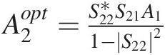
c. The delivered power is maximized when the derivative of Pdel with respect to A2 is set equal to zero (A1 is assumed fixed). Compute this derivative, solve the resulting equation, and show A2opt=S22∗S21A11−S222
 . Assume the derivative of A2∗
 with respect to A2A2 is zero.
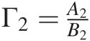
d. The complex valued reflection coefficient is defined by Γ2=A2B2
 . Use the expression in (c) to evaluate Γ2opt=A2optB2
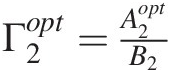 and show the result reduces for A1 fixed as in part (c) to Γ2opt=S22∗
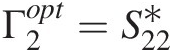 . This procedure will be used in the next chapter to derive an expression for Γ2opt
 in the case when a nonlinear component is driven with a large A1 and linear expression (3.7) does not apply.
e. Relax the assumption that A1A1 is fixed and independent of A2A2. Show that ∂A1∂A2=ΓSS121−ΓSS11
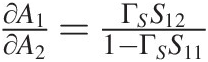 , where ΓSΓS is the source reflection coefficient. Use this result to derive the more general result, valid for nonunilateral devices: Γ2opt∗=S22+S21ΓSS121−ΓSS11
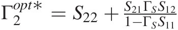


Exercise 3.6 Simpler derivation of Γ2opt=S22∗ for the case A1 fixed.
a. Start with Pdel = |B2|2 − |A2|2Pdel=B22−A22 as in the previous exercise. Without substituting the S-parameter expression for B2, differentiate with respect to A2 and show that the delivered power is maximized when dB2dA2B2∗=A2∗
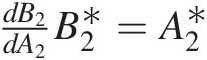 .
.
b. Divide the equation in (a) by B2∗
 and show the result is
dB2dA2=Γ2∗.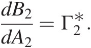
c. Now substitute the S-parameter expression for B2B2 in terms of A1A1 and A2A2, compute the derivative, and derive Γ2opt=S22∗
 .
.


References
 Findit@CUHK Library | Google Scholar
 Findit@CUHK Library | Google Scholar
 Findit@CUHK Library | Google Scholar
 Findit@CUHK Library | Google Scholar
 Findit@CUHK Library | Google Scholar
 Findit@CUHK Library | Google Scholar
 Findit@CUHK Library | Google Scholar