5.1 Introduction: Linear Equivalent Circuit Models of Transistors
This chapter introduces the major principles and methods of linear device modeling. Specifically, we present an introduction to models of transistors based on linear equivalent circuits. The equivalent circuit description attempts to associate the electrical model description with the physical structure of the device.
The models are linear in the sense we have described in detail in Chapters 1 and 3, specifically that the response of such a model to a superposition of stimuli is equal to the superposition of responses to the stimuli applied independently. As we have learned in Chapter 1, linearity implies that an RF sinusoidal signal applied at a particular frequency will produce a sinusoidal response at (only) the same frequency. We can then completely describe the linear model in terms of any one of several equivalent conventional small-signal frequency-domain descriptions, such as admittance, impedance, or scattering parameters.
Although the response of linear device models is proportional to the complex amplitudes (phasors) of the input stimuli, as with linear behavioral models, the explicit dependence on frequency of the response is not linear. That is, the response at frequency 2f is not twice the response at frequency f. Each linear circuit element contributes to the network description an admittance (or impedance, or S-parameter), a complex valued frequency-dependent number that defines the proportionality of complex-valued response to stimulus. Resistors contribute real-valued impedances independent of frequency, while ideal capacitors and inductors contribute admittances and impedances, respectively that are purely imaginary and proportional to frequency. Note that the capacitance, or the inductance, values themselves are independent of frequency. For a model composed exclusively of lumped elements, the model response is a rational function (i.e., it is given by the ratio of two polynomials) of frequency. The quantitative response also depends, of course, upon the numerical values of the elements (e.g., the resistances and capacitances).
This chapter also presents an introduction to parameter extraction. The parameters of the linear equivalent circuit model are the values (e.g., the resistance or capacitance) of each of the corresponding elements of the equivalent circuit. Parameter extraction is the process of determining the numerical values for these parameters, from measured or simulated data. The typical data used for linear RF and microwave device model parameter extraction are S-parameters. This is natural because the measurements are (ideally) linear, like the models. We will see, however, that even for purely linear microwave and RF device models, several distinct DC bias conditions must be applied. This is necessary to put the device in the appropriate operating condition for a useful linear model and to provide distinct states of device operation to help in the extraction of parasitic element values necessary to correctly determine all the device model parameters from data at the externally accessible measurement ports.
The modeling and parameter extraction processes are highly related. The full transistor model is constructed from linear electrical element building blocks (e.g., resistors and capacitors) by putting them together in a particular network – the equivalent circuit topology – in order to represent the overall device behavior. Parameter extraction is, in a rough sense, the reverse process, namely going from information at the device external terminals and using knowledge of the presumed topology to determine the numerical values of the individual electrical circuit parameters (ECPs), (e.g., the capacitance and resistance values of the primitive elements).
For this chapter we stay exclusively in the frequency domain. We will meet linear models again in Chapter 6 where we show how they arise, generally, as first-order approximations to nonlinear models in the small-signal limit. Recall we already met a particularly simple linear FET model derived from time-domain considerations in Chapter 3 (Section 3.12).
5.2 Linear Equivalent Circuit of a FET
A simple picture of a Field Effect Transistor (FET) is shown in Figure 5.1.
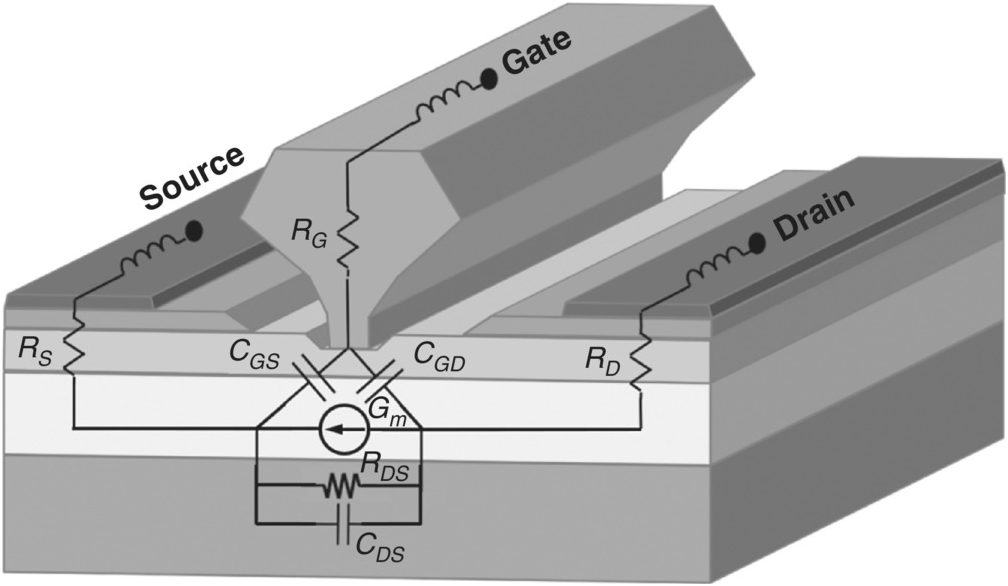
Figure 5.1 Simple FET structure with equivalent circuit elements superimposed.
Metal electrodes, labelled Source, Gate, and Drain, are shown on the top of the figure, typical of a GaAs pHEMT device (but not drawn to scale). The source and drain electrodes make ohmic contacts with a highly doped layer of semiconductor. The gate metal makes a Schottky contact with a different semiconductor layer. The active semiconductor channel, through which most of the current flows, is represented by the lighter region below. The substrate, taken as semi-insulating, is shown as the bottom layer.
The type of circuit elements and their arrangement in the equivalent circuit are consequences of our physical understanding of the device physics and its structure. The Schottky contact presents a barrier to (DC) current flow, so there is no resistor in the electrical path from the gate terminal to the channel in this simple idealization. The ohmic contacts permit current flow through the semiconductor, so there are resistances in the path from the source and drain terminals. The metal electrodes themselves are represented by inductors that affect the high-frequency RF and microwave signals. The Schottky contact sets up a built-in electric field at the gate metal-semiconductor interface that depletes charge carriers in the semiconductor depending also on the applied bias voltages at the terminals. This is modeled by parallel plate capacitors, labelled CGS and CGD. The current source element represents the main current flow in the channel and is responsible for the transistor action. Although not clear from the figure, it is electrically controlled by the local potential differences that result from applied bias conditions at the external terminals taking into account the voltage dropped across the resistors. Coupling between drain and source terminals is represented by the CDS element.
There also exists capacitive coupling among some of the physical features of the device structure that should be modeled by additional circuit elements to complete the idealized electrical model. A planar schematic that illustrates the model in somewhat more detail is shown in Figure 5.2.
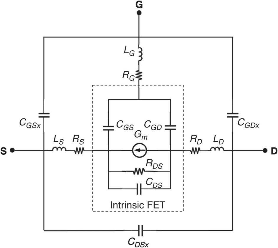
Figure 5.2 Simplified equivalent circuit of a FET with parasitic and intrinsic ECPs.
The model of Figure 5.2 is further divided into the intrinsic model, within the dashed box, with the remaining elements belonging to the extrinsic or parasitic model. The extrinsic part is represented by shells of parasitic shunt capacitance elements, within which is a shell of series-connected resistances and inductances. We will make use of this structure in the parameter extraction process. Various topologies are used [1], some more elaborate, but for simplicity, we will restrict ourselves to this.
The shunt capacitances represent metal-to-metal interelectrode parasitic effects. The resistors RS and RD, considered parasitic elements in this treatment, represent the “access resistance” – that portion of the semiconductor that is not controlled by the gate potential. The gate resistor, RG, is largely attributable to the resistance of the gate metallization. Inductances are also associated with the electrode metal and become important at high frequencies.
The intrinsic transistor is the heart of the semiconductor device. The intrinsic transistor model accounts for the bias-dependent transconductance responsible for the transistor action, channel resistance, and the bias-dependent junction capacitances. Although not visible in the structure of Figure 5.1, the physical mechanisms of self-heating, and in some cases, charge trapping, can be considered part of the intrinsic device. These phenomena are modeled by additional coupled equivalent circuits that will be introduced in Chapter 6.
5.2.1 Bias Considerations
The isolated structure of the transistor shown in Figure 5.1 provides no information about the DC operating condition at which the linear model is defined. Different device operating regimes, specified by different bias conditions, substantially affect the numerical values of the ECPs of the intrinsic model. Implicitly, this means a linear device model is defined for a specific bias condition.
Linearity requires that the ECPs do not vary with the applied RF signal. And, as these ECPs are dependent on the DC biases, these DC biases do not change with the RF signal. The DC conditions merely parameterize the linear dependence of the RF input-output relations. Since physical transistors are nonlinear components, as we learned in Chapter 1, a linear transistor model is a valid approximation to the actual device behavior provided the device is stimulated by a sufficiently small RF signal. This is why linear models of transistors are often referred to as small-signal models.
There is no precise way to know, a priori, how small such signals need to be for a linear model to be considered valid. Formal procedures for the linearization of the nonlinear equations to produce linear models in the small-signal limit are described in Chapter 6. Recall a particularly simple linear FET model was derived from time-domain considerations in Chapter 3 (Section 3.12), and ultimately converted to an S-parameter representation.
Linear device models are useful primarily to describe the device small-signal behavior in an active bias operating condition.1 At such bias conditions, we can usually neglect forward and reverse gate leakage currents, which would require a more complicated equivalent circuit representation for Figure 5.2 with additional elements. However, we will see in Section 5.5.2.1 that deliberately choosing bias conditions outside the range of normal small-signal operation can be useful for parasitic element value extraction, necessary to ultimately get the best model for simulation at the standard conditions.
5.2.2 Temperature Considerations
Temperature, analogously to bias, affects the linear equivalent circuit element values. But just as with bias, for a linear model we can usually take the device temperature to be fixed and independent of the RF signal. As long as the device is operating in the small-signal regime, this assumption is valid for most RF applications. However, as we will see in Chapter 6, there can still be a frequency-dependence to the device small-signal electrical response caused by a temperature modulation produced by a small-signal stimulus if the applied signal is varied slowly enough. Since timescales for this phenomena are typically of the order of milliseconds or longer, and the RF timescales are typically in the nanosecond range, we neglect this phenomenon in this chapter. We deal with electro-thermal considerations in Chapter 6.
5.3 Measurements for Linear Device Modeling
5.3.1 Terminal Mappings to RF Measurement Ports
The device structure and equivalent circuit shown in Figures 5.1 and 5.2 has three external terminals, one each for the gate, drain, and source, respectively. Microwave measurements are made on actual layouts – physical realizations of the transistor embedded or “wired” into a particular two-port structure. The resulting measurement data will usually be in the form of a 2 × 2 matrix, such as a two-port S-parameter or Y-parameter representation. There are several ways a two-port matrix description, and therefore the actual physical structure of the test FET for measurement purposes, can be mapped to and from the three-terminal schematic of Figure 5.2. This depends on the choice of a common terminal and the choice of the numerical ordering of the ports.
Examples of the two most common physical realizations of actual test FET layout structures, and their wiring diagrams mapping the three terminals to distinct two-port configurations, are presented in Figures 5.3–5.6 [2]. These are common source and common gate layouts, respectively, and typically have the ports ordered as shown. The relationships between the ECP values of the FET equivalent circuit and the data are completely different when the two-port parameters are provided in common source or common gate configuration.
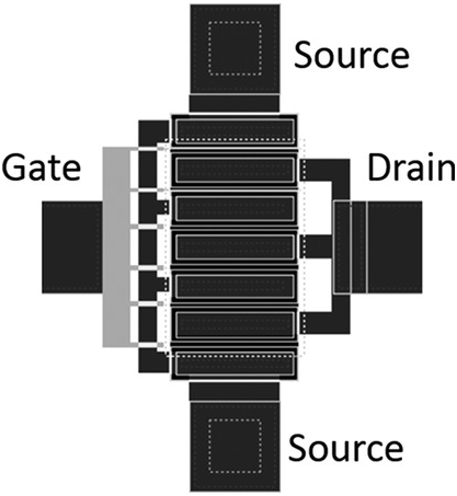
Figure 5.3 Common-source layout of a multifinger FET.
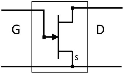
Figure 5.4 Wiring diagram of a three-terminal device consistent with the common-source layout of Figure 5.3. Port one is the gate and port two is the drain.
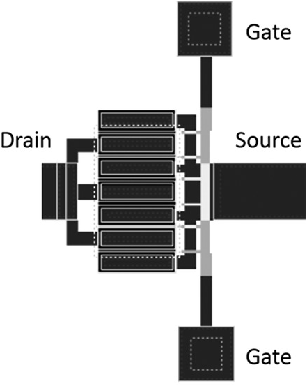
Figure 5.5 Common-gate layout.
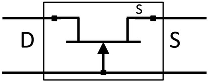
Figure 5.6 Wiring diagram of a three-terminal model corresponding to the common-gate layout of Figure 5.5. Port one is the drain and port two is the source.
To make this point more concrete, imagine, for the moment, that we can neglect the inductances and resistances in the extrinsic equivalent circuit of Figure 5.2. We could then identify each intrinsic ECP from the two-port parameters in either common source or common gate configuration. For example, the formula for the feedback capacitance, CGD, in terms of common source Y-parameters is given in (5.1) and the corresponding formula in terms of common-gate Y-parameters is shown in (5.2), where the superscripts are used to label the respective two-port configuration. The formulas (5.1) and (5.2) correspond to the port orderings specified in the diagrams of Figures 5.3–5.6. Other port orderings lead to different but related formulas. In the Appendix we show explicit formulas to relate these descriptions under ideal circumstances.
 (5.1)
(5.1) (5.2)
(5.2)It is therefore essential for parameter extraction to know the particular two-port realization of the physical device, including the ordering of the ports.
5.4 On-Wafer Measurements and Calibration
Transistor S-parameters for modeling purposes are best made on-wafer using vector network analyzers (VNA). A typical test bench is shown in Figure 5.7. A semi-automated wafer probe station is shown with a wafer, micro-manipulators for probing, microwave ground-signal-ground (GSG) probes and a microscope for visualization. A 50 GHz VNA with built-in sources is visible behind the probe station. Bias voltages are controlled and monitored with multiple source monitor units (SMUs) as shown on the left. A temperature controller is also shown that is used to set the temperature of the chuck on which the wafer is placed, providing controllable thermal boundary conditions for the transistor.

Figure 5.7 Test bench for S-parameter measurements for modeling.
5.4.1 Linear Device Modeling Flow
The linear modeling flow is the process of making well-calibrated microwave measurements on one or more FET test patterns and using the information to obtain the ECPs for the corresponding model, sometimes including the geometrical scaling rules for the ECPs in the process.
5.4.1.1 Test FET Layout
A typical common source layout of a 6 finger by 50 μm (6 × 50) test FET structure for modeling and extraction is shown in Figure 5.8. The test structure contains more than just the FET. It contains ground-signal-ground pads (at the extreme left and right) for on-wafer probing and carefully designed nearly 50 Ω transmission lines (the narrow structures attached to the signal pads) to achieve single-mode EM wave propagation for the microwave signals to the device.
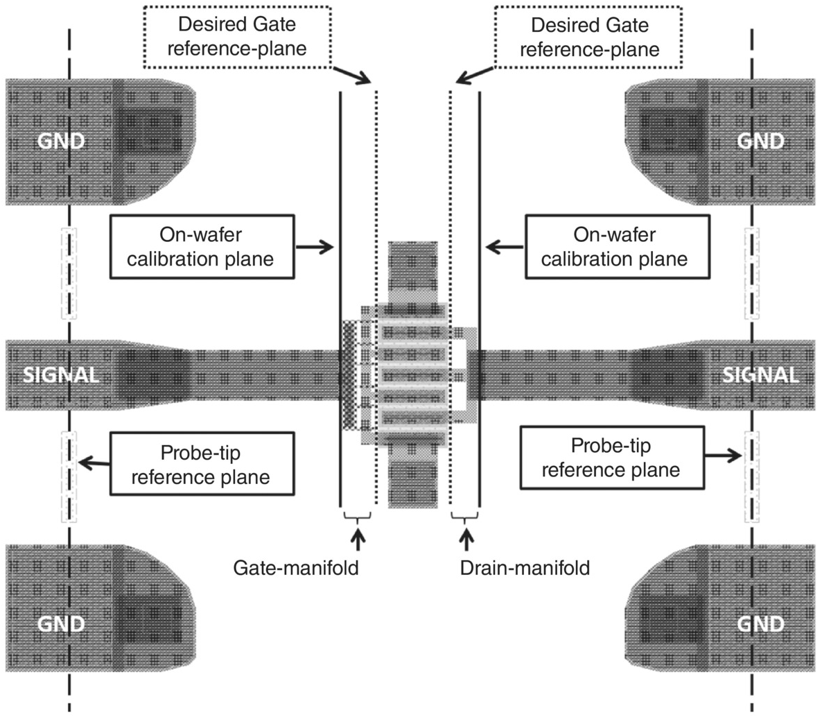
Figure 5.8 Test FET pattern for model extraction of a common-source FET.
The S-parameter (and DC) measurements at the probe tips represent the characteristics of the entire structure. In an actual circuit, say a MMIC, the pads and transmission lines are not present. It is therefore essential to characterize and model just the device at the well-defined reference planes where the component is defined, so that the model representing the device can be placed into a circuit for design purposes.
5.4.1.2 Calibration
Calibration, for RF and microwave network analysis measurements, is a very important topic, but will only be summarized briefly here. More details can be found in [3–5]. Poorly calibrated measurements lead to poor models. On-wafer calibration standards are usually best [4], and we will restrict ourselves to this approach.
We need well-calibrated S-parameters at the on-wafer calibration planes of Figure 5.8. The best way to do this is to define on-wafer calibration standards that can be used to move the reference planes from the probe tips to these planes. Four calibration patterns, defining known short, open, load, and thru (SOLT) standards, for RF and microwave calibrations, are shown in Figure 5.9.

Figure 5.9 On-wafer patterns used to help characterize the FET device embedded in the layout of Figure 5.8.
The pads and transmission lines are identical to those of the FET test pattern of Figure 5.8. The first three standards are placed at the calibration planes the same distance apart as in the test FET structure. Only the “zero-delay” thru pattern is different for relative probe placement – the ports are physically closer together so the calibrations planes coincide – since this is a precise way to generate a good thru standard.
The S-parameters from the four patterns of Figure 5.9 are measured, and used together with the measured S-parameters of the test FET layout of Figure 5.8, to determine the S-parameters at the device reference planes. Algorithms are built into modern VNA software that use these four SOLT standards and the test structure measurements to return the S-parameters at the device planes. Alternative sets of on-wafer calibration patterns can be used with different calibration algorithms (e.g., LRRM or multiline TRL methods) to accomplish the same objectives [4].
5.4.1.3 Gate and Drain Manifolds
Before we can move the reference planes to the desired gate and drain boundaries indicated by the dotted lines in Figure 5.8, we must account for the behavior of the port manifolds.
The manifolds are the feed structures between the solid and dotted lines that couple the signals from the ends of the transmission lines of the test structure to the multiple gates and drain bars of the transistor. These structures are implemented very differently when a FET is physically realized as part of a MMIC design, for example. The idea is to model the manifolds of the test structure to move the reference planes and define the device at the dotted lines. The model we will ultimately build and extract, in this and the next chapter, will be for this device between the dotted lines of Figure 5.8. It will be incumbent on the MMIC designer to account for any parasitic effects introduced by the design-specific coupling of this device to others in the circuit, including the multiple gate and drain connections.
The gate manifold, in the layout of Figure 5.8, has source metal crossing over gate metal, with an interlayer dielectric in between. This could be modeled as a set of parasitic capacitors for each crossover and additional capacitors for fringing fields and the vertical bar of metal just to the right of the left solid line of Figure 5.8. A preferred modern approach, however, is to represent the manifold behavior by S-parameters computed directly from the layout using electromagnetic simulations. It is usually sufficient to simulate a 2-port S-parameter matrix with an input port at the calibration plane and an output port corresponding to an effective single gate finger at the inner (device) plane.2 A similar simulation from layout can be done for the drain manifold.
With each manifold characterized in terms of its respective two-port S-parameters, simple linear de-embedding methods are used to move the reference planes to the desired device planes – the inner dotted lines in Figure 5.8.
5.5 The Device
The S-parameter data, now transformed to the device planes, are indicative of the transistor – not the test structure – and so the data are in as close as possible correspondence to the idealized structural representation of Figure 5.2.
5.5.1 Parasitic Shells of Series Impedances and Shunt Capacitances
The topology of Figure 5.2 can be abstracted to that of Figure 5.10, evidencing nested shells of fixed ECPs around the bias-dependent core of the intrinsic model. From a specific common terminal set of S-parameters, this suggests a conceptually simple method of parasitic stripping using linear algebra, by identifying generic Y- and Z- shells of parasitic elements of Figure 5.10 in the extrinsic topology of Figure 5.2 [6,7].

Figure 5.10 Device topology emphasizing Y–Z shells plus intrinsic device.
The common-source two-port S-parameters describing the device are a set of four complex numbers at each measured frequency. Certainly, at any fixed, single frequency, there are far too many ECPs in the device topology of Figure 5.2 and equivalent Figure 5.10 to be identified from these four numbers. Even using data over a wide range of frequencies, it is not practical to directly estimate the values of all extrinsic and intrinsic elements at a typical active bias condition where the linear device model is most likely to be useful. It is at this point we appeal to additional knowledge of the device behavior in certain distinct regions of operation in order to help us with the parameter extraction.
5.5.2 Parasitic Shell “Stripping”
5.5.2.1 Using Bias Conditions to Simplify the Equivalent Circuit for Parasitic Element Extraction from Measurements
Due to the significant dependence on bias of the intrinsic ECPs, the topology of the intrinsic device can be simplified in specific “cold FET” conditions, where the transistor is not active. The total topology of the device model in Figure 5.10 then becomes more amenable to unambiguous extraction, where the parasitic elements can be more readily separated from the intrinsic elements. Under these conditions, the parasitic elements in the different shells of Figure 5.10 can be identified much more easily.
5.5.2.2 Identification of the Parasitic Capacitances
We consider one of the cold FET conditions where VDSDC = 0VDSDC=0 and the device is reverse-biased to the point where the gate-source voltage is less than the threshold voltage, VGSDC<VT . Under these conditions, where the device is not active, the device intrinsic transconductance, GmGm must vanish. Under this strong reverse bias condition, we can also assume the intrinsic drain-source resistance, RDSRDS, is large enough to be neglected, which removes both of those branches from the equivalent circuit of the intrinsic device. If we further limit the characterization frequency range for the S-parameters to be far below the cutoff frequency of the device, we can also usually neglect the series inductances, and since we are ultimately interested in the imaginary part of the admittance elements in the outer shell, we can neglect the series resistances as well. The inductances and resistances will be dealt with by considering a different bias condition in Section 5.5.2.4. This assumes the value of intrinsic CDSCDS is zero at this particular bias condition.
We are left, therefore, with the combination of outer-shell parasitic capacitances in parallel with the intrinsic device junction capacitances at this reversed bias condition. This simple approximate equivalent circuit topology is shown in Figure 5.11.

Figure 5.11 Simplified parasitic capacitance model of a FET under passive bias condition for parasitic capacitance identification.
Given the topology of the Figure 5.11, the correspondence between the 2-port linear data and the desired ECPs is most easily formulated in the admittance representation. We use the standard formula to convert the S-parameters to the Y-parameters given by (5.3), which follows from (3.36).
 (5.3)
(5.3)The following simple relationships defining the element values in Figure 5.11 in terms of the common source Y-parameters are given in equations (5.4).
 (5.4)
(5.4)Here CGSi and CGDiCGSiandCGDi are the intrinsic capacitances of the junction at the particular cold bias point, and CGSx, CGDx, and CDSxCGSx,CGDx,andCDSx are the parasitic values that, being assumed independent of bias, are to be identified.
There are still too many unknown parameters (five) on the left side of equations (5.4), to identify them all from one set of device admittances. Therefore, we characterize an array of devices of physically scaled layouts, shown in Figure 5.12, of various numbers of parallel gate fingers with various finger widths, and use the resulting geometrically dependent ECP values to separate parasitic from intrinsic element values.

Figure 5.12 FET array of scaled layouts to identify parasitic elements.
Fitting the first equation of (5.4), from data for each set of devices with the same number of fingers separately, we get the plots of Figure 5.13 where the intercepts (extrapolation to zero width) provide the values for the parasitic capacitances of devices with different numbers of fingers. This interpretation assumes that the intrinsic capacitance values, extrapolated to zero gate width are zero. This is a physically reasonable approximation neglecting only fringing fields and perimeter effects that are usually insignificant for practical FET geometries.

Figure 5.13 Linear regression allows for parasitic capacitance identification.
It is a good sanity check that the slopes of the three independently fitted lines plotted in Figure 5.13, are so consistent.
Plotting the values of CGSxCGSx versus the number of fingers, we obtain the geometrical scaling rule from the linear fit shown in Figure 5.14.

Figure 5.14 Scaling rule for shunt parasitic gate-source capacitance versus finger number.
A similar approach can be taken for the remaining parasitic elements in Figure 5.11.
5.5.2.3 Stripping Off the Outer Admittance Shell
With the parasitic capacitance values of the outer parasitic shell now known, the two-port description at the device plane can be moved to the plane of the parasitic impedances.
Given the topological representation of these parasitics, the relationship between the common source two-port parameters at the Y and Z planes can be expressed most simply according to (5.5). The subtraction is element by element in the admittance representation, and it gives the common-source Y-parameters with the parasitic capacitances removed (Figure 5.15). The inverse of this difference is, therefore, the Z-parameter matrix, Z, at the plane of the series parasitics.
 (5.5)
(5.5)In (5.5), we have computed the common source parasitic admittance matrix, YparaYpara, in terms of the parasitic capacitance elements using the definition of the admittance matrix according to (5.6) and the structure of Figure 5.2.
 (5.6)
(5.6)
5.5.2.4 Parasitic Resistance and Inductance Extraction
We now move on to extracting the series parasitic shell containing the resistances and inductances. The strategy is similar to the capacitance parasitic extraction step of 5.5.2.2, in that we choose a bias condition to simplify the equivalent circuit, but this time the operating conditions are quite different. We will also do a matrix subtraction to remove the parasitic elements, but this time, due to the topology, we do so in the impedance domain.
Direct Method Based on Extreme Forward Bias Condition
A significantly forward-biased gate voltage is chosen such that there is substantial current flowing into the gate terminal across the Schottky barrier. The drain-source voltage is chosen to be zero, or, nearly equivalently, the drain current is biased to be equal and opposite to half the gate current. That is, IDDC=−IGDC2 . This condition forces the drain and source current to be equal.
This DC condition is assumed to be sufficiently extreme so as to effectively short out the Schottky barrier junction, interpreted as a strongly forward biased diode with, therefore, a very large conductance. The large conductance presents an effective electrical short between this intrinsic gate node and any other node to which it is connected in the intrinsic equivalent circuit. That is, the entire intrinsic FET can be collapsed to a single node, reducing the equivalent circuit topology within the Z-shell to a simple T-topology shown in Figure 5.16.

Figure 5.16 Idealized highly forward-biased FET equivalent circuit after the capacitance shell is stripped off. The intrinsic FET is assumed to be shorted out.
We remind the reader that gate current was not explicitly accounted for in the simple equivalent circuit of Figure 5.2. We assume a large conductance only at this stage in order to identify the series parasitic elements. The final linear model will be valid only for conditions where the actual gate leakage is negligible.
From Figure 5.16, we note only six equivalent circuit elements, all series parasitic elements, remain in the total model topology, now that the parasitic capacitances have been stripped off and the intrinsic device collapsed to a point at this bias condition. These EPCs can therefore be directly identified from the real and imaginary parts of the Z-matrix of the data at this plane. This follows from the computation of the parasitic Z-matrix, given in (5.7) in common source configuration, which follows from the definition (5.8), applied to the circuit representation of Figure 5.16.
 (5.7)
(5.7) (5.8)
(5.8)While formally (5.7) can be solved for the six ECPs at any frequency by taking simple linear combinations of the real and imaginary parts of the Z-matrix, the frequency of the measurements must be high enough to measure the inductances without too much uncertainty. A fit to (5.7) from data over a range of moderate-to-high frequencies generally provides a more robust extraction than a direct solution from data at a single CW frequency.
This method has the following drawbacks, however. The extreme forward bias condition may be too stressful for modern short gate-length devices, causing damage during the measurements. Since RD and RS, are physically semiconductor access resistances, and as such can be current dependent, their extraction from data at an extreme bias condition may yield parameter values that might be different from their actual values under more normal operating conditions.
Modified Procedure at Less Extreme Forward Bias
A method that is potentially more accurate, but also more complicated, than that of 5.5.2.4.1, is presented in reference works [8–10]. In this case, the gate bias is only slightly forward biased, just enough to get the channel as open as possible but at much less extreme forward current conditions through the gate than 5.5.2.4.1. The intrinsic device is therefore not completely shorted out and an approximate modeling of its composition is required. The equivalent circuit of the series parasitics and the intrinsic device at this bias condition is shown in Figure 5.17 [1,10].

The parameters R1 and C1R1andC1 are associated with the total gate intrinsic resistance and capacitance, respectively, and RchRch represents the active channel resistance at this bias condition. The fractional factors of RchRch come from an analysis of the device as a distributed structure [11,12]. In this three-terminal schematic, the contribution of the seemingly strange −Rch6 factor at the gate with the Rch2
 factors at the drain and source are equivalent to the more familiar common-source Z-parameters reported in the literature. The value of RchRch has to be estimated from data on other test structures, and its value depends on the material properties of the semiconductor. The authors use 1.55e-4 ohm-meter for GaAs and 6.75e-4 ohm-meter for GaN. Values of R1 and C1R1andC1, along with the other six parameters in the impedance shell, are then optimized to fit the measured Z-parameters over a wide frequency range. More detailed considerations can be found in [1].
By applying either the methodology of Section 5.5.2.4.1 or that of 5.5.2.4.2, or equivalent, over the FET array of sizes, one can extract the values and the geometrical scaling rules for the parasitic elements. The data from an array of layouts and the resulting scaling rule for the drain resistance, RD, of a GaAs FET is given in Figure 5.18.

Figure 5.18 Dependence of the parasitic drain resistance as a function of total gate width, as fitted to data from devices of multiple layouts.
Similar results are found for the source resistance.
A similar analysis leads to the gate resistance, RG, but its scaling rule is quite different.
5.5.2.5 Gate Resistance Scaling
Geometrical Argument
From an examination of the common-source layout of Figure 5.3, given that the gate current flows along the fingers from left to right, we would expect, from simple geometrical arguments, the gate resistance to increase roughly linearly with the width per finger, w, for a fixed number, N, of parallel gate fingers.3 For the same value of w, the resistance should scale inversely with N, because the fingers are arranged in parallel. The total gate width, Wtot, is just the product of the width per finger and the number of fingers, so we have Wtot = N ⋅ wWtot=N⋅w. From these considerations we derive a simple gate resistance scaling rule according to (5.9) with parameters α≈1α≈1 and β≈2β≈2. Here the ref superscript refers to the values of a particular reference device. Note how different the rule for gate resistance scaling is compared to that of the source and drain resistance, the latter given by a simple expression such as shown in Figure 5.18. The rule (5.9) enables the estimation of the gate resistance for a range of geometries specified in terms of total gate width, Wtot, and number of parallel gate fingers, N. This can be simply re-expressed in terms of the width-per-finger, w, if desired (see Exercise 5.7). Obviously, care must be used to properly interpret the meaning of the geometrical parameters that define the device.
 (5.9)
(5.9)Empirical Results
Alternatively, an approach similar to that of 5.5.2.4 for the drain and source resistances can be followed for the gate resistance to arrive at an empirical expression for the gate resistance, RG, as a function of the total gate width and the number of parallel gate fingers. The results are shown for a pHEMT process in Figure 5.19. While the scaled RG values move in the same direction with Wtot and N as predicted by (5.9) for positive exponent values, the actual best fit values for the exponents are different. The data and parameter values are shown in Figure 5.19.

5.5.3 Stripping Off the Series Parasitics
The task is now to transform the two-port data through the parasitic Z-network to get to the intrinsic transistor.
The relationship of the intrinsic model linear two-port parameters (represented by the rectangular block within the parasitic impedances in Figure 5.11) to the two-port parameters after stripping the parasitics of the series impedances is most conveniently expressed by the simple relation (5.10), with ZparaZpara as given by (5.7):
5.6 Intrinsic Linear Model
Now we are, finally, at the intrinsic equivalent circuit. The common source intrinsic linear equivalent circuit for a FET is shown in Figure 5.20. This neglects, as stated previously, leakage current through the gate as may happen at large reverse or forward bias conditions. It also neglects resistive elements, denoted RGS (sometimes labeled Ri) and RGD, elements in series with the junction capacitances, and also a phase associated with a time-delay of the transconductance. We will analyze an intrinsic model augmented with these elements in Section 5.6.5.

Figure 5.20 Intrinsic FET equivalent circuit after parasitic shell stripping.
The topology of the intrinsic FET is seen from Figure 5.20 to be just a parallel combination of resistors and capacitors. We can easily compute the intrinsic model common source admittance matrix in terms of the individual ECPs in the equivalent circuit using the definition (5.6). The result is given in (5.11), with GDS=1RDS . The hard part was all the work needed to move the reference planes for the various two-port description from the calibration plane all the way to the intrinsic device plane to arrive at the simple intrinsic model.
 (5.11)
5.6.1 Consistency Check of Linear Model Assumptions
Since conductances and capacitances from lumped elements are all real numbers, inspection of (5.11) reveals that the intrinsic FET model admittance matrix is a sum of a real part that is frequency independent and an imaginary part that is linearly dependent on frequency. That is, the intrinsic equivalent circuit topology predicts an especially simple explicit dependence on frequency. This prediction can be experimentally tested by de-embedding the measured (extrinsic) S-parameter data through the parasitic network and plotting the real and imaginary parts of the intrinsic admittance parameters as functions of frequency. Some examples of intrinsic admittance parameters for a GaAs FET capacitances are shown in Figures 5.21 and 5.22.

Figure 5.21 Measured imaginary part of intrinsic Y11 vs frequency of a GaAs FET.

The behavior of the intrinsic input admittance data versus frequency is a validation of the appropriateness of the equivalent circuit as a model of the transistor’s linear behavior. It confirms that the reactive elements present in the gate-source and gate-drain branches are indeed two capacitances with different values.
5.6.2 Identification of Intrinsic Linear Equivalent Circuit Elements
Each of the elements of the common-source intrinsic admittance matrix (5.11) is a simple linear combination of resistive and capacitance terms. It is evidently possible to invert these equations and solve uniquely and explicitly for each of the equivalent circuit elements in terms of simple linear combinations of the intrinsic common-source admittance matrix elements. These equations are given in (5.12)–(5.16), where we drop the superscript int for intrinsic.
 (5.14)
 (5.15)
 (5.16)
5.6.3 Discussion and Implications
Model consistency means the right-hand sides (RHS) of (5.12)–(5.16) should end up being independent of frequency even though the numerators and denominators are themselves frequency dependent. This will never be exactly true in practice, but the validity is quite good for most FETs over much of the useful operating frequency range, provided the parasitic elements are properly identified and de-embedded from good measurements, as we demonstrate in the next section.
5.6.3.1 Problems Caused by Poor Parasitic Element Extraction
The following example illustrates what happens when there is a poor extraction of the parasitic element values. Broadband S-parameters are measured at a particular active bias condition for a GaN HFET. The device is a 0.15 μm × 6 finger × 60 μm GaN HFET with individual source vias from Raytheon Integrated Defense Systems [13]. The device is optimized for 1–40 GHz operation for applications including power amplifiers, low noise amplifiers, and switch applications. All further examples of GaN transistors in this chapter are based on this device.
The parasitic shells are stripped away using the methods of 5.5.2.4. The resulting intrinsic elements are computed, at each frequency, using the formulas (5.12)–(5.16). The resulting element values versus frequency are plotted for selected elements for two different values of the parasitic source inductance, LG in Figure 5.23.

Figure 5.23 Flatness with frequency of intrinsic ECPs of a GaN HFET device for two values of parasitic inductance, LG. The bias condition is VGS = −1.8 V and VDS = 20 V. The device is a 0.15 μm × 6 finger × 60 μm GaN HFET with individual source vias from Raytheon Integrated Defense Systems [13]. The device is optimized for 1–40 GHz operation for applications including power amplifiers, low noise amplifiers, and switch applications.
The frequency dependence of the intrinsic elements is much flatter over the wide range of the measurements with the (correct) smaller value of LGLG. While this example may strike the reader as somewhat extreme, the gate inductance can be difficult to obtain without a large uncertainty. However, it evidently has a significant effect on the frequency flatness of the computed intrinsic elements. Flatness with frequency can be used as an optimization objective in more sophisticated (but more complicated) approaches to the total extraction problem. See for example [14].
With the correct values of the parasitic elements determined, the intrinsic ECPs of the model at each operating point can be determined from the small-signal intrinsic Y-parameters using (5.12)–(5.16) at a single frequency, provided the frequency is not so low that there is large uncertainty in elements, such as capacitances. Examining the capacitance values in Figure 5.23, we see large fluctuations in values below 5 GHz, indicating we should choose a higher frequency for the extraction point. Beyond about 30 GHz we observe an increasing spread in the values versus frequency. So in this case, we choose 10 GHz to be the extraction frequency.
The proof that the model topology and the parameter extraction methodology described here produce accurate linear models is shown in Figures 5.24 and 5.25. In these figures, the broadband measured S-parameters on the 6 × 60 μm GaN HFET are compared with the linear model simulations at two different bias conditions. The fit is quite good over the full range from 0.5 GHz to 50 GHz for both bias conditions, even though the identification of the ECPs for the intrinsic model were identified at only the single CW frequency of 10 GHz. There is a slight discrepancy visible between the measurements and simulations for mid-frequency S11 and S22 and the mid-to-high-frequency gain, S21, is slightly underestimated by the model. A more advanced model will be presented in Section 5.6.4 that improves upon these results.


Figure 5.25 Broadband validation of the linear model of the 6 × 60 μm GaN HFET. Measured (symbols), modeled (lines). Frequency range is 0.5–50 GHz. DC bias conditions: VGS = −1.2 V, VDS = 6 V. The model ECPs were identified at 10 GHz.
An important implication of (5.12)–(5.16) is that the identification of the element values can be done at any single CW measurement frequency. This is the principle of “direct extraction” that has become standard industry practice since the late 1980s [6,7]. That is, once it is established that (5.16) is essentially independent of frequency, the particular fixed value of the ECPs can be obtained by a spot measurement at a single CW frequency.
Of course, in practice the extraction frequency must be high enough for the S-parameters at the calibration plane to register a capacitance contribution, but not so high that the data at the intrinsic transistor becomes overly sensitive to additional distributed effects or errors in the parasitic element value extraction (such as the port inductances).
In principle, for a given bias condition, there is an optimum value of frequency for identifying the element values from (5.12) to (5.16). Detailed considerations including uncertainty analysis are presented in [15,16].
The model of Figure 5.20 effectively compresses the independent measurement data from a great many frequencies, into only five real numbers, specifically the values of Gm, GDS, CGS, CGD, and CDS. These five numbers are predictive of the broadband frequency performance of the intrinsic device through the model. Even including the parasitic elements, the complete linear model is an extremely compact representation of the DUT frequency behavior at the given DC bias point.
Another consequence of the predictive power of the model is that the model can be used to extrapolate beyond the measurement data used to identify the element values. We can identify the element values using (5.12)–(5.16) at any one frequency, say 10 GHz, (or over a moderate range of frequencies, say 5–20 GHz) and then simulate with the model at a CW frequency of, say, 50 GHz. Recall the model frequency performance is determined completely from the element values and their arrangement in the circuit topology. So a well-extracted model will work well until the simulation frequency is so high the device topology is no longer valid. Predictions of DUT performance up to a large fraction of the transistor cutoff frequency, fT, are reliable if the model parameter extraction has been done properly. Moreover, such simulations can be more accurate than an actual measurement at the desired high frequency. Of course this depends on the instrument measurement bandwidth and the quality of the test transistor layout and calibration patterns. Nevertheless, transistor figures of merit (FOM) such as fT and fmax, can often be obtained more reliably and much less expensively by first extracting, from high-quality medium frequency data, a model of the device and then simulating with the model at frequencies higher than those used for the extraction to compute the FOM. In fact, this is often the way these device FOMs are defined.
5.6.4 A New Element Revealed from the Data
The above treatment followed from the postulated linear equivalent circuit model of Figure 5.20. There are five elements in this equivalent circuit, yet there are eight real numbers associated with the intrinsic small-signal parameters – the two-port matrix description in any representation – admittance, impedance, or scattering, etc., at any one frequency. An examination of the imaginary part of the intrinsic model admittance (5.11) shows that the off-diagonal matrix elements of the imaginary part are equal and proportional to frequency. But let’s plot the measured imaginary parts of the off-diagonal admittance elements and compare them. This is shown in Figure 5.26 for the same 6 × 60 μm GaN HFET device as above at the DC bias of VGS = −1.8 V and VDS = 20 V.

Figure 5.26 Measured off-diagonal elements (symbols) and linear fit (lines) of the 6 × 60 μm GaN HFET intrinsic input admittance in common source configuration.
The frequency dependence is (approximately) linear for each of the two imaginary terms, so they can be interpreted (modeled) as capacitances. But they are clearly not equal as the simple intrinsic model of Figure 5.20 predicts. So we must re-visit our equivalent circuit model and add a new element!
In formal analogy with the transconductance, we place the transcapacitance element in the drain-source branch, and represent it by a symbol of a capacitor surrounded by a circle. The augmented equivalent circuit diagram and the corresponding common-source intrinsic admittance are shown in Figure 5.27 and (5.17), respectively.

The corresponding identification formula for the new element is easily defined according to (5.17) in terms of the common-source intrinsic admittance matrix elements.
 (5.17)
The complete common-source intrinsic admittance matrix corresponding to the augmented equivalent circuit is given in (5.18). The transcapacitance element shows up in the second row of the first column in the second matrix of (5.18).
 (5.18)
It should be emphasized that this element, or an equivalent to be discussed presently, is required for improved model accuracy at (nearly) any frequency compared to the five-element model of Figure 5.20, because it was specifically identified, through (5.17), to account for the measured difference of the intrinsic off-diagonal matrix elements.
To prove this point, we show the result of the linear model based on the addition of the transcapacitance element, using Figure 5.27 as the augmented intrinsic model by adding the transcapacitance element. Comparing Figure 5.28 to that of Figure 5.24, we observe the augmented model fits S11 and S21 better, especially at mid-to-high frequencies, and fits mid-frequency S22 better as well. It does appear that S22 at the highest frequencies may agree slightly less well than the simpler model, but we must remember that the measurement uncertainty is also greatest at 50 GHz.

Figure 5.28 Broadband validation of the linear model of the 6 × 60 μm GaN HFET with the transcapacitance element (model of Figure 5.27). Measured (symbols), modeled (lines). Frequency range is 0.5–50 GHz. DC bias: VGS = −1.8 V, VDS = 20 V. The ECPs of the model were identified at 10 GHz.
A more discriminating comparison between the models, with and without the transcapacitance element, can be observed by plotting separately the magnitudes and phases of the extrinsic S-parameters of each model and comparing them to the corresponding S-parameter data. This is done in Figures 5.29 and 5.30.


Figure 5.30 S21 and S22 versus frequency: Measured (symbols) versus model with the transcapacitance (solid line) and without the transcapacitance (dashed lines). Frequency range is 0.5–50 GHz. DC bias conditions: VGS = −1.8 V, VDS = 20 V. The ECPs of the model were identified at 10 GHz.
5.6.4.1 Discussion
The use of a transcapacitance element brings with it some complications, however, one of which will be described now. The magnitude of the transadmittance, (5.18), of the intrinsic model increases without bounds as the stimulus frequency increases due to the transcapacitance element. This follows from the small-signal relationship (5.19), deduced from (5.18) by calculating the magnitude of the drain current response to a perturbation in the gate-source voltage. The parameter ττ is defined as the ratio of the magnitude of the transcapacitance to the transconductance. Fortunately, the terminal resistances RG and RS, in conjunction with the intrinsic gate capacitances, produce an input time constant that provides a frequency limit beyond which the intrinsic transadmittance won’t increase. The overall model is, therefore, generally quite accurate up to a significant fraction of the transistor cutoff frequency. Nevertheless, the high-frequency behavior of (5.19), even for an intrinsic control frequency limited by input charging time constants, may not follow the measured and physically required decrease with frequency of the transadmittance at extremely high frequencies.
 (5.19)
At the DC bias point VGS = −1.8 V, VDS = 20 V, the model parameter values are Cm = − 110 fFCm=−110fF and Gm = 0.075 SGm=0.075S, so τ = 1.5 psτ=1.5ps. Even at 50 GHz, ωτ = 0.47ωτ=0.47, and the square root factor is only 1.1, so things still work well.
For linear models, there is a classical approach that associates a time-delay with the transconductance element that can account for the measureable behavior shown in Figure 5.26 without the need for a transcapacitance element. This will be described in Section 5.6.5.1. The time-delay approach is not as easily generalized to the large-signal case as the transcapacitance approach, however. We will return to the transcapacitance issues in Chapter 6 when we discuss the large-signal model.
5.6.5 Related Linear Models
5.6.5.1 Model with Time-Delay of the Transconductance
Historically, another parameter had long been introduced to deal with the imaginary part of the nonreciprocity of the off-diagonal intrinsic admittance parameters for linear models. The most common approach is a time-delay associated with the transconductance element. The frequency-domain representation of a time-delay is a complex number on the unit circle with a phase proportional to the frequency, where the delay parameter, ττ, is the coefficient of proportionality. The ττ parameter varies with the DC bias just like the other intrinsic ECPs. The circuit diagram, with this term added, is shown in Figure 5.31 with the corresponding admittance matrix representation in (5.20).
 (5.20)
The new model parameter is now the time-delay, τ. The relationship between (5.18) and (5.20) can be understood by expanding the exponential of (5.20) in orders of ωτ.
 (5.21)
So the transcapacitance of (5.18) can be interpreted as a first order approximation to the delay of the transcondctance. Alternatively, the Cm value can be identified from data using the formula of (5.17) and used to solve for the parameter τ in (5.20) using the second equation of (5.21).

As discussed in Section 5.6.4.1, this is still a good approximation even at 50 GHz. Given the improved results using the transcapacitance demonstrated in Figures 5.29 and 5.30, it is clear the model is quite improved over this frequency range.
5.6.5.2 Adding RGS and RGD Elements
The intrinsic models of Figures 5.27 and 5.31 have six elements, each of which can be determined from a simple closed-form expression involving the intrinsic Y-parameters from data at any CW frequency. Since there are 8 (real) parameters in the 2×2 intrinsic Y-parameters, we might well ask if there are another two circuit elements that can be identified from the remaining 2 real parameters that could further improve the model. The answer is generally yes. Contrary to what is predicted by (5.18) and (5.20), the measured real parts of Y11 and Y12 are not exactly zero, and the measured imaginary parts are not exactly proportional to frequency. These facts suggest we might be able to add a resistor to each of the gate-source and gate-drain branches to improve the model agreement with the measurements.
From any single frequency measurement, it would not be possible to decide whether these new resistors should be placed in series with the input capacitances or in parallel. Over a broad frequency range, however, for bias conditions for which there is negligible gate leakage, the series combination fits the frequency-dependent data much better. The corresponding model appears in Figure 5.32. This choice can be seen as a natural consequence of good data analysis. There is also a physically based interpretation for these resistors, namely that the displacement current through the gate must go through some of the resistive semiconductor channel before appearing at either intrinsic source or drain terminal.

Figure 5.32 Eight-element intrinsic linear FET model.
The two new elements require a modification of the formulas expressing the eight ECPs as explicit linear combinations of the intrinsic Y-parameters. We do this in a two-step process. We define the following linear combinations of common-source Y-parameters shown in (5.22). The expressions for each element, shown in (5.23), follow from simple algebra [6].
 (5.22)
 (5.23)
The expressions for CGS and CGDCGSandCGD in (5.23) reduce to those of (5.15) and (5.14), respectively, in the low-frequency limit. However, those of (5.23) are more sensitive to noisy data or if the data is affected by DC leakage at the measurement condition.
For some active bias conditions, the actual values of CGD are so small that to accurately resolve the RGD element in series with it, a stimulus frequency either beyond the measurement BW of conventional VNAs is required, or else the large uncertainty in the extracted RGD element value can reduce the usefulness of this model. In such cases, it may be better to put the RGD element in parallel with CGD. (keeping RGS in series with CGS). In this case, RGD represents DC gate-drain leakage. While this makes for a model with an asymmetric equivalent circuit topology, we must remember that the active bias condition itself “breaks the symmetry” of the device structure, so this presents no problem for a linear model where the element values are fixed.
5.7 Bias-Dependence of Linear Models
We now return to the DC bias dependence of the linear model. This will help with the transition to the large-signal model in Chapter 6. We assume the relations (5.12)–(5.16) hold for “all” bias conditions, making explicit the dependence not only on frequency but on bias. For example, the bias-dependence of the CGS and CGD elements are given by (5.24) (compare (5.15) and (5.14). A plot of these circuit element values as a function of the DC gate and drain bias voltages is given in Figure 5.33.
 (5.24)
Figure 5.33 Bias-dependent junction capacitances of a GaAs pHEMT defined by (5.24). VGS varies from −2 V to −1.2 V in 0.2 V steps in the direction of the arrows. The bias conditions are those applied to the extrinsic terminals.
We notice several interesting features of these characteristics. Each capacitance, CGS and CGD, depends in a complicated nonlinear way on both DC bias voltages, VGS and VDS. This is not so surprising in itself, based on the previous considerations articulated in this chapter. But the conventional definition of a two-terminal capacitor has a capacitance that depends only on the single voltage difference between the two terminals. We will have to come back to the circuit theory – and also to the physics – required to model this multiple voltage dependence. We will do this in Chapter 6.
From Figure 5.33, we see that for VDS values greater than about 1.5 V, the actual measured value of the feedback capacitance CGD decreases as the gate voltage increases. That is, the capacitance, CGD, at pinchoff (VGS = −2 V) is larger than when the channel is partially opened by increasing the gate voltage. It is interesting to note that CGD exhibits exactly the opposite dependence on gate voltage, VGS, compared to the behavior of capacitance CGS, and indeed opposite to the conventional dependence of depletion capacitance on the applied voltage. Linear models with capacitance values that do not change with DC bias conditions consistent with these data will necessarily result in simulations that disagree with actual device behavior.
We also note that as VDS approaches zero, the gate voltage dependence of both CGS and CGD becomes the same, and even the numerical values of the two capacitances become nearly the same. This is a manifestation of the drain-source symmetry of the intrinsic transistor. A more complete treatment of device symmetry, for all bias voltages, is presented in Chapter 6.
5.7.1 Bias-Dependent Linear Models
Simple bias-dependent linear models can be easily implemented in commercial simulators. The models are built as subcircuits using standard circuit elements configured in topologies like Figure 5.2 with intrinsic and parasitic elements. A typical symbol associated with such a model is given in Figure 5.34.

Figure 5.34 Symbol for scalable bias-dependent linear FET model.
The model takes as input the two independent DC port voltages needed to determine the ECP values of the intrinsic model, and the two independent geometrical parameters such as the total gate width and number of parallel gate fingers for the scaling rules of both the parasitic elements and the intrinsic ECPs. In this case, a fifth input is the name of a file containing the bias-dependent intrinsic element values tabulated as a function of both bias voltages. Since the DC voltages correspond to the extrinsic terminals they remain on a grid if they were characterized on a grid. This means the data can be stored in standard tables readable by the simulator. The simulator also interpolates the values should the requested bias conditions not coincide with the discrete data points. For geometrical scaling the extracted algebraic rules for the parasitics are simply evaluated using the expressions developed and fit during the extraction process. The intrinsic elements scale proportionally to the ratio of the total gate width of the desired structure to that of the reference device.
5.7.1.1 Limitations of Simple Geometrical Scaling Rules
The geometrical scaling rules introduced above are only approximate. They hold over a certain range of layouts, or, equivalently, values of the scaling ratio, r. Simple scaling starts to break down at very high frequencies, where device distributed effects become important for large finger widths.4
Thermal Issues
Another limitation of simple geometrical scaling rules for the electrical component values of linear (and nonlinear) models is caused by thermal effects. Two identically biased FETs with the same DC power density (power per unit gate width) will differ in their “junction temperature” if the effective thermal resistance per unit gate width is different. This can be the case when one device uses more fingers in parallel compared to a second device that uses fewer but wider fingers. The multiple interior gate fingers see different local thermal boundary conditions, and therefore generally get hotter than the exterior fingers. Moreover, simple approximate analysis indicates that thermal resistance scales sublinearly with the inverse of the total gate width [17]. Since temperature affects the equivalent circuit element values – especially those of the intrinsic device, it is generally important to have at least a rough understanding of the geometrical scaling properties of the thermal resistance (and heat capacitance).
A practical approach for linear device models is to carefully model several layouts, say small, medium, and large, and “scale locally” around each layout. It is of course critical for first-time success that any FET actually used in a MMIC design be realized as a properly scaled version of the layout used for the device model! Otherwise, a unique layout may introduce an unanticipated – usually undesirable – performance characteristic when the circuit is actually fabricated.
5.7.1.2 DC Bias Conditions Are Not Computed
It is important to understand that the DC input parameters must be supplied by the user and are not related to the DC operating point computed by the simulator (unlike a general large-signal model). So if the transistor of interest is embedded in a circuit with a lossy path from the bias supplies, the designer must estimate the actual terminal voltages the device will see and provide the correct, actual terminal voltage differences for the device through the model instance of Figure 5.34.
5.8 Summary
Linear equivalent circuit models of devices were introduced starting from physical considerations of the transistor structures. Microwave FETs were used as examples. The models are linear in the sense that the output RF signals are proportional to the input signals, and therefore they relate complex input phasors to complex output phasors at the same frequency. The ECPs of a linear model don’t vary with the impressed RF signal. The frequency dependence of a complete linear model depends on the type of primitive electrical elements and their arrangement in the equivalent circuit topology. The models are predictive in the sense that the broadband frequency dependence, at a fixed DC operating point, is determined by only a few numbers, namely the value of the equivalent circuit elements.
Parameter extraction schemes were introduced for FET linear models, based on S-parameter data taken at different bias conditions in order to help separate the parasitic elements of the device from the bias-dependent elements associated with the intrinsic transistor. Measurements on an array of different scaled layouts were shown to also be necessary to discriminate all the ECPs based on their dependence on gate width and number of parallel gate fingers. This procedure also provided geometrical scaling rules enabling the resulting model to predict the performance of FETs with different number of fingers and total gate widths. The final model also provided more accurate simulated broadband linear frequency behavior because the parasitic elements were properly determined and, therefore, so were the intrinsic bias-dependent ECPs.
Explicit formulae were developed for the intrinsic ECPs of standard intrinsic models with 8 or fewer elements. For these models, the individual component element values can be identified in terms of measured, de-embedded single-frequency S-parameter data, once the parasitic element values in the topology are known.
The bias-dependence of intrinsic ECPs reveals interesting relationships among the elements that must be properly accounted for in nonlinear models. We will return to this in Chapter 6.
5.9 Exercises
Exercise 5.1 Derive the expression for the Y-shell parasitic capacitances from the Figure 5.2 using the definition (5.6).
Exercise 5.2 Show that the bias condition IDDC=−IGDC2 forces the drain and source currents to be equal.
Exercise 5.3 Using the definition of the admittance matrix in equation (5.6), derive (5.11) from the equivalent circuit in Figure 5.20.
Exercise 5.5 Derive (5.2) from (5.11) and the appendix that relates common source and common gate admittances. Derive expressions for the other four element values in the linear equivalent circuit of Figure 5.20 in terms of their common-gate intrinsic admittance parameters.
Modify the formulas for the element values in terms of common-gate admittance parameters with the introduction of the transcapacitance element introduced in 5.6.4.
Exercise 5.6 Derive (5.22) and (5.23) for the 8-element FET model of Figure 5.32.
Exercise 5.7 Derive the ideal scaling rule (5.9) with α = 1α=1 and β = 2β=2, for the gate resistance as a function of total gate width, Wtot, and the number of parallel gate fingers, N. Derive an equivalent expression in terms of the width-per-finger, w, and N.
References
 Findit@CUHK Library | Google Scholar
 Findit@CUHK Library | Google Scholar
 Findit@CUHK Library | Google Scholar
 Findit@CUHK Library | Google Scholar
 Findit@CUHK Library | Google Scholar
 Findit@CUHK Library | Google Scholar
 Findit@CUHK Library | Google Scholar
 Findit@CUHK Library | Google Scholar
 Findit@CUHK Library | Google Scholar
 Findit@CUHK Library | Google Scholar
 Findit@CUHK Library | Google Scholar
 Findit@CUHK Library | Google Scholar
 Findit@CUHK Library | Google Scholar
 Findit@CUHK Library | Google Scholar
 Findit@CUHK Library | Google Scholar
 Findit@CUHK Library | Google Scholar
 Findit@CUHK Library | Google Scholar