Many important concepts regarding nonlinear microwave systems and an extensive discussion of nonlinear device modeling techniques were introduced in previous chapters. Now, to summarize what we have learned and to facilitate the comprehension of the presented concepts, this chapter illustrates how accurate nonlinear device models and circuit simulators can be used in the design of microwave circuits. For these purposes, the design of a typical medium-power amplifier (PA) circuit will be used as an example.
We show that the effort of considering nonlinear circuit simulation and active device models is justified as these tools reduce the complexity, and thus the time needed for practical circuit designs and their characterization. Moreover, these device and circuit representations enable the analysis of the circuit’s operation, not only via the input-output observation, as is done in the laboratory, but also via looking into every internal equivalent circuit node of the active device.
The chapter is organized in two major thematic parts.
The first part, consisting of Section 7.1, recalls some results of active device modeling from previous chapters, explaining the importance and impact they have on the predicted power amplifier behavior. Special attention will be paid to the model features that determine the most important PA characteristics: output power, drain efficiency, and AM/AM and AM/PM distortion, i.e., gain amplitude and phase profiles.
The second part, Section 7.2, details the PA computer-aided design and verification procedures. It first illustrates the roles that the nonlinear device model and a simulator can play in the various circuit design steps, constituting an aid, or even a substitute, to the laborious and expensive measurement-intensive conventional PA design procedure. Then, we will also show how simulations can be used to estimate and interpret the performance characteristics of the implemented circuit.
7.1 Nonlinear Device Modeling in RF/Microwave Circuit Design
Contrary to a low-noise amplifier, or a low-power PA design, which, nowadays, often use MMIC implementation, medium to high-power PAs rely on packaged devices mounted in a PCB. Therefore, not only do the equivalent circuit models of Chapters 5 and 6 have to be embedded in a more or less complex package model, but the designer may also face the situation of having to design a PA with a device for which there is still no available model provided by the device vendor. This is quite common in mobile communications base station design, and is aggravated in high-power (hundreds of watts peak-power) circuits whose active devices are often internally prematched. This is one field in which the frontier between active device modeling and circuit design is blurred, and so where the microwave engineer has to make a prudent choice of the best compromise between a model’s complexity (and, thus, difficulty of extraction) and accuracy, i.e., mostly the model’s capability to predict the actual device’s output power and efficiency load-pull contours and AM/AM and AM/PM profiles. As we will see, this goes all the way from the judicious choice of the equivalent circuit topology to the formulations of the iDS(vGS,vDS), Qgs(vGS,vDS), Qgd(vGS,vDS) and Qds(vGS,vDS) nonlinear constitutive relations.
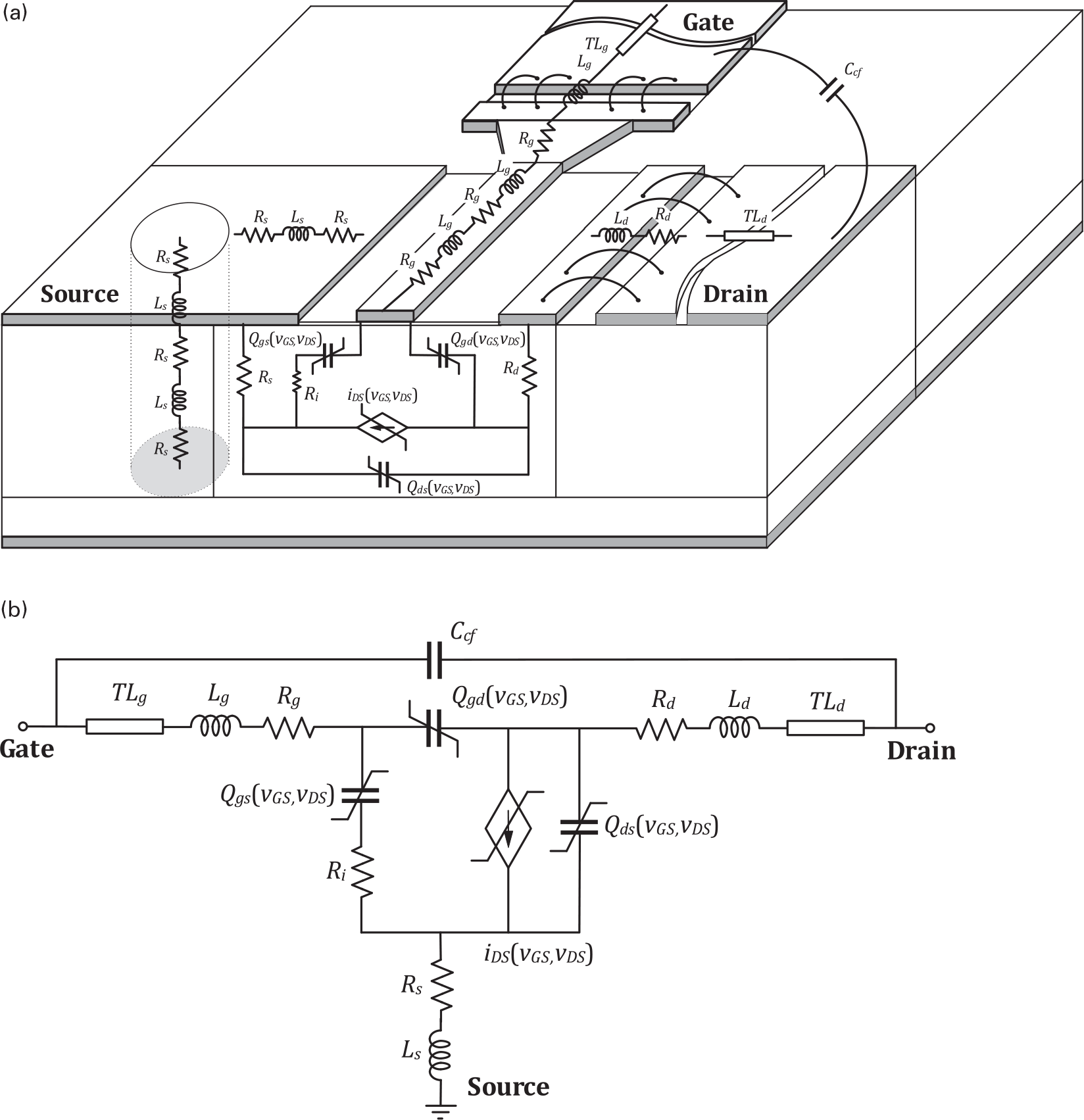
To obtain a representation as close as possible to the real device, the model topology is frequently established according to our knowledge of the device’s structure and physical operation. Actually, Figure. 7.1(a) is an illustration of the geometry of an RF MOSFET, which is then translated into the equivalent circuit model of Figure 7.1(b). As discussed in Chapters 5 and 6, this model can be divided into intrinsic and extrinsic subcircuits. The former ones are associated with the channel, while the latter are the representation of the parasitic effects associated to the metallization of the die and the package.
7.1.1 The Extrinsic Subcircuit Model
Since the extrinsic elements are bias-independent, or linear, we could think that they may not be as important as the intrinsic elements for the design of a nonlinear circuit such as a power amplifier. However, these extrinsic elements play a fundamental role in the accurate prediction of output power and efficiency load-pull contours. To illustrate this, Figure 7.2 shows three different sets of load-pull contours for a commercial 240 W packaged Si LDMOS device. Figure 7.2(a) depicts the obtained load-pull predictions in which the used model is only composed of the adopted FET iDS(vGS,vDS) nonlinear model; (b) shows the updated load-pull predictions – reported at the intrinsic reference plane – when the intrinsic Qgs(vGS,vDS), Qds(vGS,vDS) and Qgd(vGS,vDS) nonlinear voltage-dependent charge models or their equivalent capacitances, Cgs(vGS,vDS), Cds(vGS,vDS), and Cgd(vGS,vDS), were also included; and, (c) illustrates the final load-pull predictions of the entire model of Figure 7.1, i.e., when also the extrinsic sub-circuit is considered.
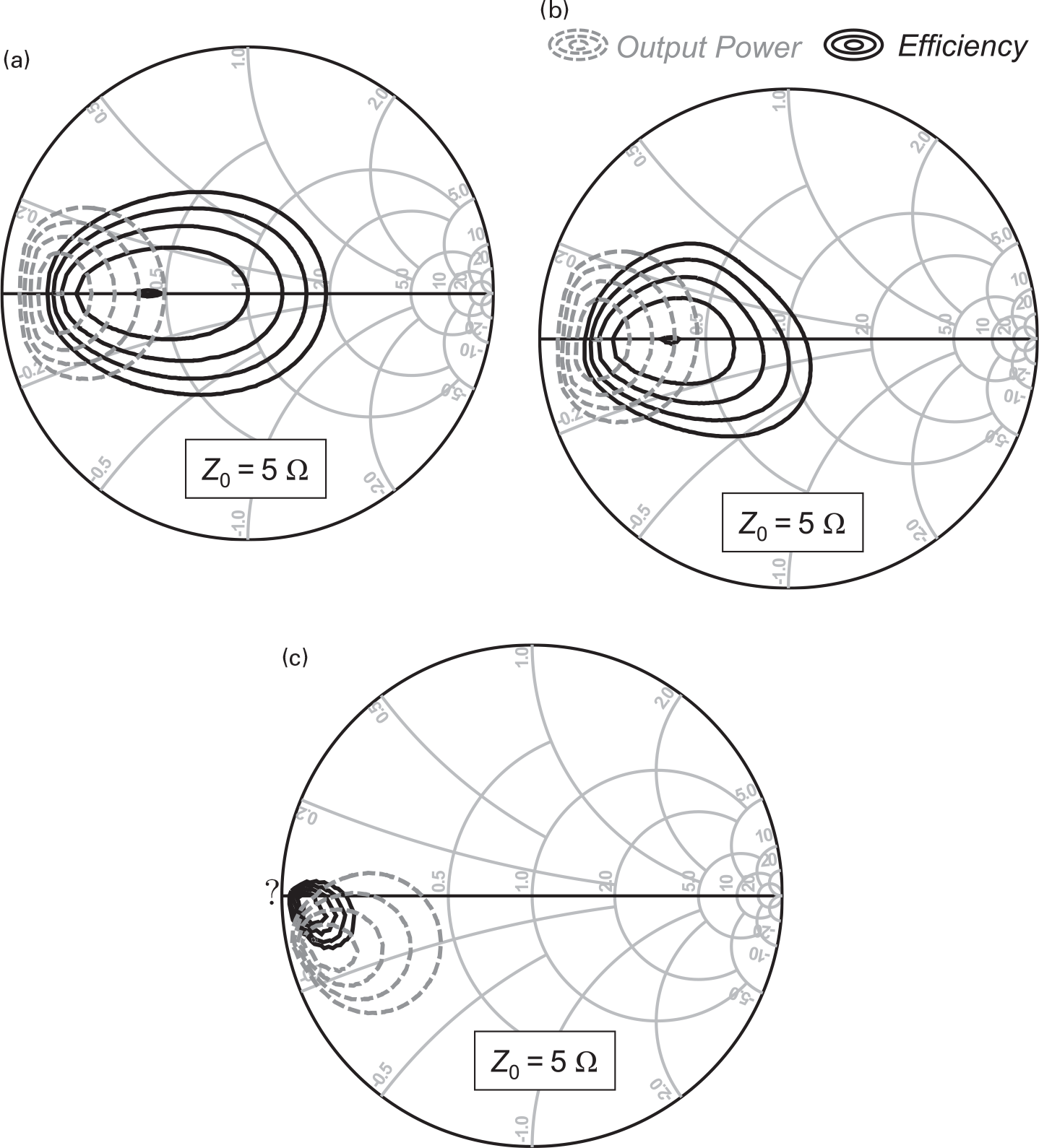
Figure 7.2 Output power and efficiency load-pull contours of a 240 W packaged Si LDMOS device simulated at 1800 MHz in three different situations: (a) considering only the adopted FET iDS(vGS,vDS) nonlinear model, (b) considering the FET iDS(vGS,vDS) and Cgs(vGS,vDS), Cds(vGS,vDS) and Cgd(vGS,vDS) intrinsic nonlinear capacitances at the intrinsic reference plane, and (c) considering the entire model, i.e., also including the extrinsic linear elements.
Comparing the contours of Figure 7.2(b) and (c) with those determined by the nonlinear FET channel current of (a), first we should note a non-uniform stretching of the contours, in particular in high impedance values, where the output voltage excursion is higher, producing a large variation of the nonlinear output capacitance. Thus, after de-embedding the small-signal capacitance, the optimum impedances become more reactive. Finally, with the inclusion of the extrinsic elements in (c), the load-pull contours moved to a different Smith chart region.
Measuring the load-pull contours at the extrinsic reference plane, so that they can be used as a practical power amplifier design tool, usually requires a very complicated and time-consuming task of laboratory load-pull characterization. However, if we had access to a complete equivalent circuit model, we could obtain these load-pull contours through simulation, or simply determine their estimates at the intrinsic level [1,2] and then calculate their extrinsic counterparts, embedding the impedance transformation effects of the extrinsic subcircuit elements. Alternatively, the power amplifier design could be done at the intrinsic reference plane incorporating all extrinsic components into the matching networks.
The extraction of the package parasitic network requires S-parameter characterization of a dummy device, i.e., an empty package, and/or measurements of a complete device biased at extreme quiescent states, such as cut-off, or gate-channel junction forward bias at the FET’s triode region.
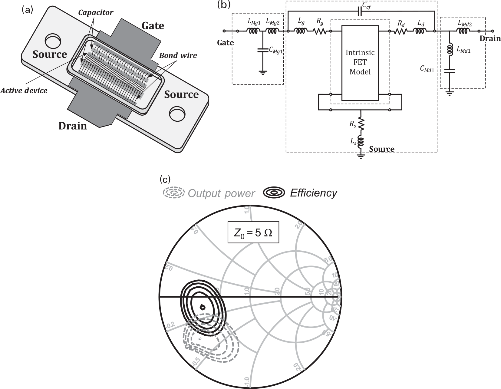
In high-power devices, as represented by the illustration presented in Figure 7.3(a), the intrinsic optimum impedances are so low that in-package prematching networks are often needed to transform them into manageable impedance values at the package reference plane. Unfortunately, the physical dimensions of these multifinger devices and of their connection pads, bond-wires, leads and prematching structures are often an appreciable fraction of the wavelength. Therefore, their accurate modeling cannot be accomplished with lumped elements, requiring, instead, complex electromagnetic simulations [3]. The obtained S-matrices – or their time-domain equivalent circuit representation [4] – are then included into the entire high-power device model, as illustrated in Figure 7.3(b). With these intricate prematching structures, the external reference plane moves further away from the intrinsic one, which produces a larger transformation of the load-pull contours, as shown in Figure 7.3(c). Moreover, the narrowband nature of these prematching networks strongly influences the harmonic impedances at the intrinsic reference plane, regardless of the harmonic terminations provided at the package terminals; and this significantly limits the use of harmonic manipulation for optimized PA performance.
7.1.2 Nonlinear iDS(vGS,vDS) Current Model
After prescribing the equivalent circuit topology, we now need to discuss the intrinsic elements. Of these, a realistic voltage-dependent iDS(vGS,vDS) drain current model is key for an accurate prediction of the AM/AM profile and the output power and drain efficiency load-pull contours. As explained in Chapter 6, various model formulations can be adopted, from more or less compact formulae, to complex, but systematic, neural networks. However, more important than the actual iDS(vGS,vDS) formulation is the measurement dataset from which it is extracted.
7.1.2.1 iDS(vGS,vDS) Current Model Extraction
In devices that suffer from obvious thermal, or even trapping, effects, such as power FETs, dc and RF data are not consistent [5]. Hence, either we have an NVNA to measure the device in a wide set of operating conditions [6] and then rely on the simultaneous nonlinear optimization of dc and drive-level and load dependent RF data described in Chapter 6, or we try more conventional data collection procedures such as bias-dependent S-parameter data. In that case, iDS current is obtained by integration of the transconductance Gm(vGS,vDS) and output admittance Gds(vGS,vDS) profiles measured under pulsed bias conditions.
As an example, in Figure 7.4 we can observe pulsed dc I/V curves, from a GaN HEMT device, and the ones obtained from the Gm and Gds integration over vGS and vDS, when the applied pulses were incapable of producing isodynamic measurements. As expected, if the thermal and trapping states are not the same for all tested bias points, the obtained I/V curves will be different, being impossible to fit these measurements to any single iDS(vGS,vDS) model expression.
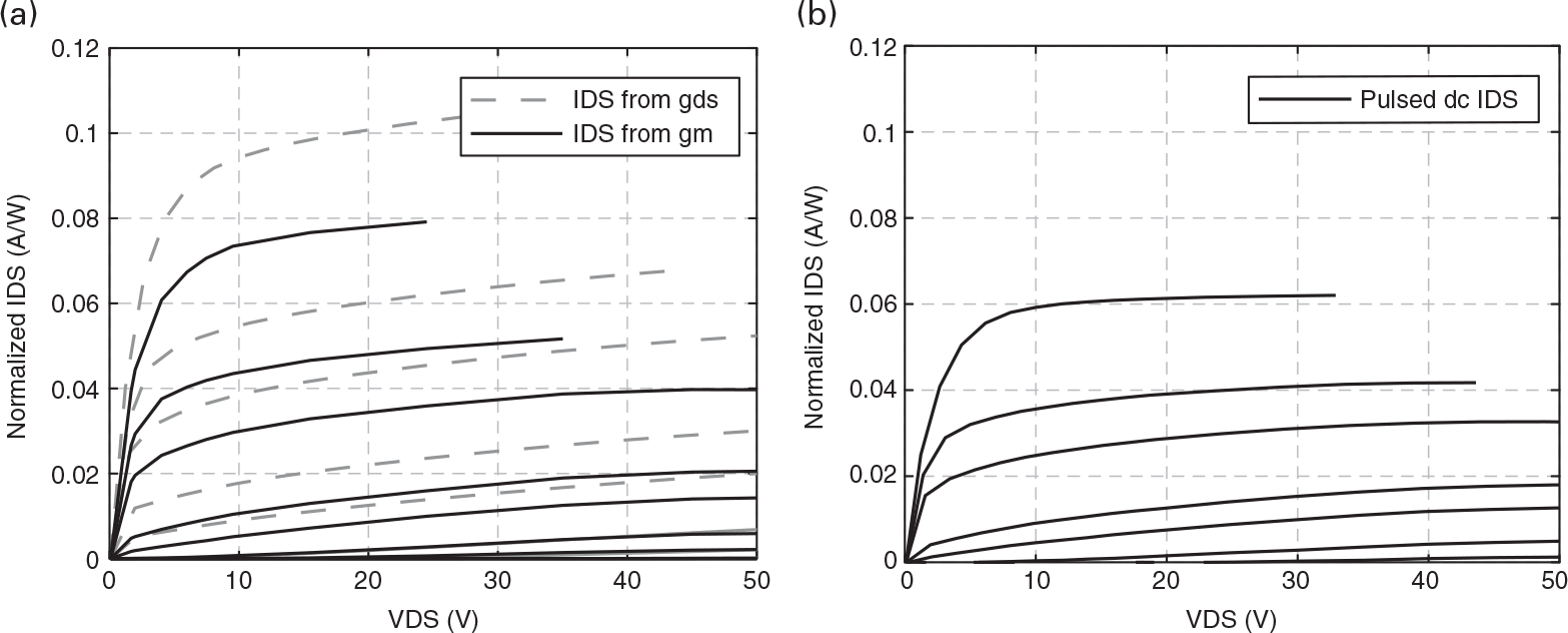
On the contrary, if a prepulse is used to set the traps’ state, guaranteeing that the thermal and trapping states do not change for all measured bias points [7] – obtaining, this way, isodynamic measurements – the I/V curves will be the same, either directly measured from the iDS pulses, or obtained from the Gm and Gds integration, as shown in Figure 7.5.
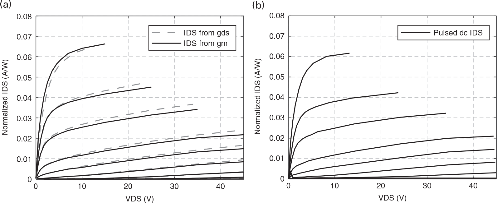
Figure 7.5 I/V curves of a GaN HEMT device (a) obtained by Gm(vGS,vDS) and Gds(vGS,vDS) integration – referred to as “IDS from gm” and “IDS from gds”, respectively – and (b) with the direct pulsed I/V method, when the measurements are guaranteed to be isodynamic.
7.1.2.2 Impact of the iDS(vGS,vDS) Current on the PA Output Power and Efficiency
The knowledge obtained from modeling these thermal and trapping effects also helps us to understand how they affect the I/V curves, which may guide us later during our PA design.
For instance, it is known that, when a high vDS peak voltage is applied to the device, the maximum iDS current, IMAX, decreases and a threshold voltage, VT, displacement is observed due to the trapping effects [5–8]. Consequently, the iDS(vGS,vDS) curves will be different if we consider the I/V curves pulsed from 0 V or from a high peak quiescent voltage, which, in turn, will modify the optimum power and efficiency load terminations, as show in Figure 7.6(a).
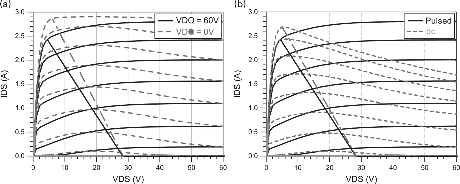
Figure 7.6 Illustration of the (a) trapping and (b) thermal effects’ impact on the optimum power load estimation.
Thermal effects will also produce an IMAX drop when the device operates in large-signal mode, because of the increased device’s dissipation and temperature, and thus decreased channel conductivity [9]. Therefore, if we only consider the I/V curves measured at room temperature, the estimation of the optimum power and efficiency impedances could also be different from the real ones obtained when the high-power signal is applied to the device, and thus its temperature is increased, as illustrated in Figure 7.6(b).
7.1.2.3 Impact of the iDS(vGS,vDS) Current on the PA AM/AM Distortion
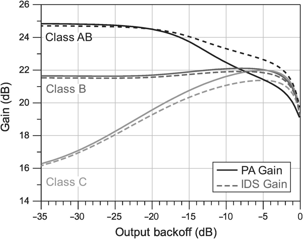
Having discussed the implications of the iDS(vGS,vDS) drain current model on the maximum output power and efficiency, we will now take a look at the distortion arising from this nonlinear voltage-controlled current source. For that, we will remove the nonlinear intrinsic capacitances – i.e., replace them by their linear versions – and compare the simulation results with the ones obtained when the full nonlinear model is considered.
Figure 7.7 shows this comparison for three different PA operation classes corresponding to shallow class AB, class B, and shallow class C. Looking into these results, we can conclude that the nonlinear iDS(vGS,vDS) current is, indeed, the main contributor to the AM/AM characteristic of a PA, because only slight differences are observed due to the input and output mismatches produced by the nonlinear capacitances. Actually, in [10] it is explained how each of these curve shapes can be related to particular iDS(vGS,vDS) model features such as the FET’s soft turn-on and its saturation to triode region transition.
7.1.3 Nonlinear Intrinsic Capacitance Models
7.1.3.1 Nonlinear Capacitance Models Extraction
The problems experienced with the iDS(vGS,vDS) model extraction, which were related to the thermal and trapping effects, are also present in the identification of the intrinsic nonlinear voltage-dependent charge sources. Therefore, to guarantee an isodynamic extraction, the double-pulse bias-dependent S-parameter measurements we adopted for the iDS model extraction should still be used for the capacitances.
Figure 7.8 shows typical Cgs(vGS,vDS), Cds(vGS,vDS), and Cgd(vGS,vDS) profiles. A high variation with vGS is observed in the Cgs profile around the threshold voltage, whereas Cgd and Cds only present a significant variation – with vGD and vDS voltages, respectively – when the device becomes operated in the triode region.
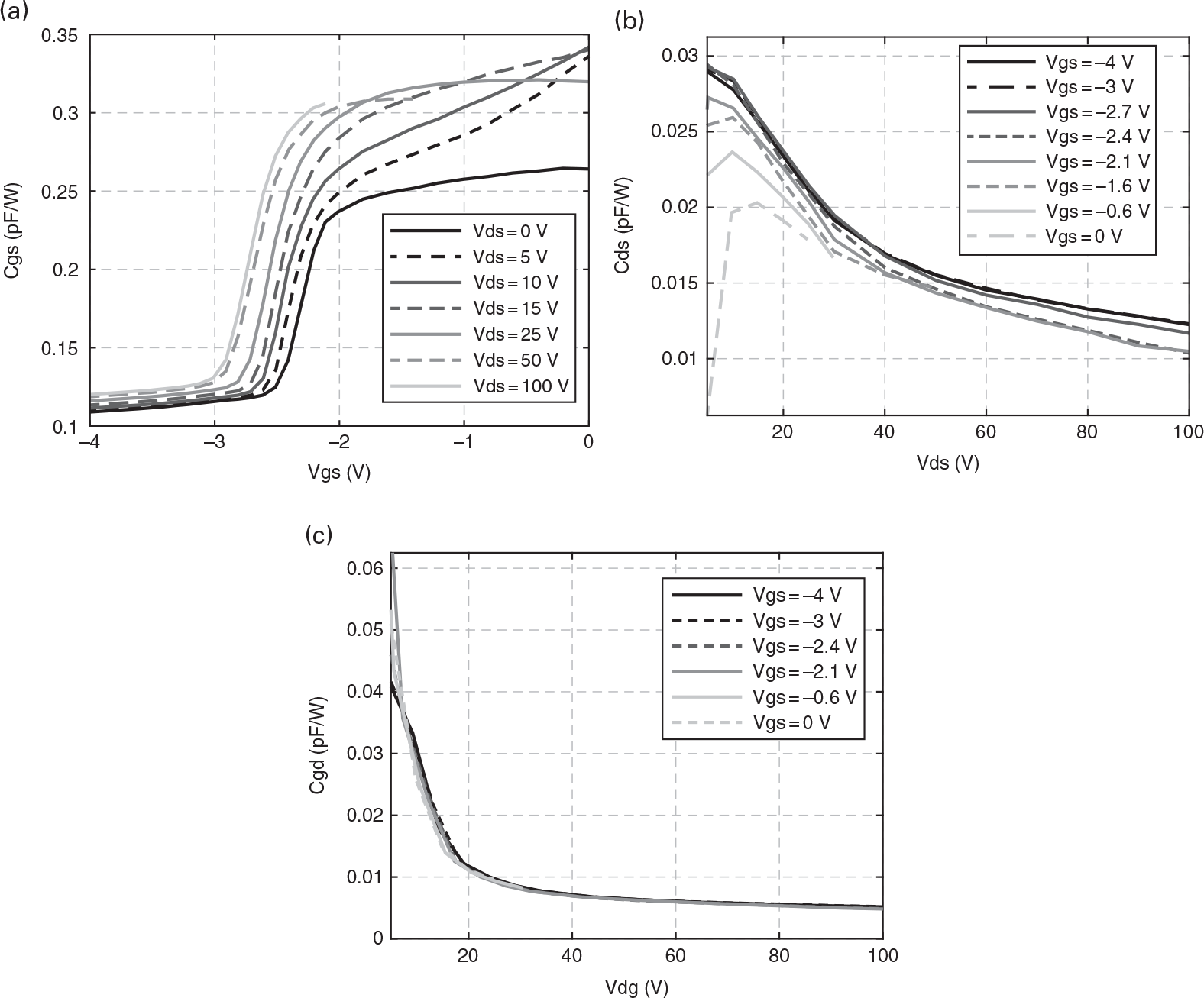
These variations will detune the output efficiency load-pull contours predicted when only the I/V curves are considered, as was seen in Figure 7.2. In addition, for advanced PA architectures, such as the Doherty PA, where it is necessary to compensate the delay between the main and auxiliary amplifiers [11], the variation of these capacitances will make it more difficult to determine the correct delay that should be used for large-signal operation. Moreover, these variations will have a severe impact on the AM/PM PA characteristic, as we will explain next. Consequently, the nonlinearity of the intrinsic capacitances and their accurate modeling should be also taken into account for a successful PA design.
7.1.3.2 Impact of the Intrinsic Capacitances on the PA AM/AM and AM/PM Distortion
With respect to the nonlinear distortion induced by the intrinsic capacitances, we have to distinguish the PAs based on the Si LDMOS and GaN HEMT, the two main RF power transistor technologies used for mobile communication base stations, since they present significant differences in their normalized capacitances. Si LDMOS devices usually have higher Cgs and Cds capacitances and lower Cgd feedback capacitance, when compared with those of GaN HEMTs [12].
Another aspect that we should take into consideration when assessing the impact of Cgd nonlinearity in the PA performance is that this can be viewed as two independent effects. On one hand, Cgd is a nonlinearity in itself because, as seen Figure 7.8(c), it manifests a noticeable variation with the vGD voltage. But, on the other hand, it should be noted that, even if Cgd were linear (i.e., constant or bias independent), it would still constitute a source of nonlinearity. Because Cgd is reflected, through the Miller effect, to the input as Cgd(1 − Av), and to the output as Cgd(Av − 1)/Av, and the voltage gain, Av, will have to vary due to the inevitable PA gain compression, the effect of Cgd will also be nonlinear. Measurements and simulations of microwave FET amplifier circuits have shown that, perhaps unexpectedly, the input Miller reflected Cgd nonlinearity is more significant than the direct Cgd(vGD) nonlinearity [10].
To understand the underlying reasons for this surprising result, equation (7.1) gives the value of the intrinsic vgs voltage when the PA is excited by a sine wave of amplitude Vs(ω). Because the equivalent nonlinear capacitance that appears at the FET’s input terminals is composed by this input Miller reflected Cgd along with the nonlinear Cgs(vGS) capacitance, the intrinsic Vgs phasor voltage will vary, in amplitude and phase, with the amplitude drive, A, according to
 (7.1)
(7.1)where Cgs0 is the time-varying Cgs(t) averaged over one RF period [10].
Figures 7.9 and 7.10 show the normalized (in a per watt basis) Cgs0 and the Cgd,Miller dependence with the amplitude for Si LDMOS and GaN HEMT based PAs, respectively. The selected VGS bias points were the ones corresponding to the same three operation classes used for the iDS(vGS,vDS) distortion analysis. Although both PAs present similar capacitance profile shapes, the input Miller reflected Cgd value for Si LDMOS PAs is almost insignificant when compared with the Cgs0, whereas in the GaN HEMT PAs it is the major contributor to the input capacitance variation. This means that in GaN HEMT PAs, the input capacitance decreases whenever the gain compresses or it increases when a gain expansion is observed.
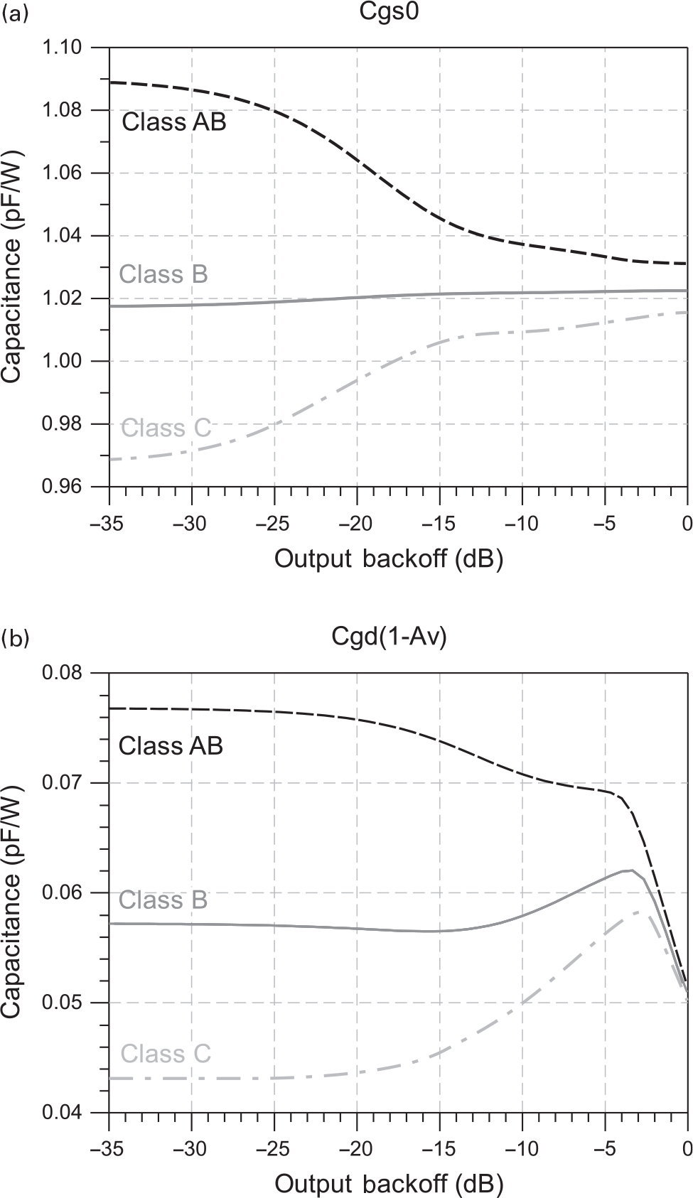
Figure 7.9 Normalized (per Watt) profiles of (a) the Cgs0 component and (b) the input Miller reflected Cgd for a Si LDMOS based PA.
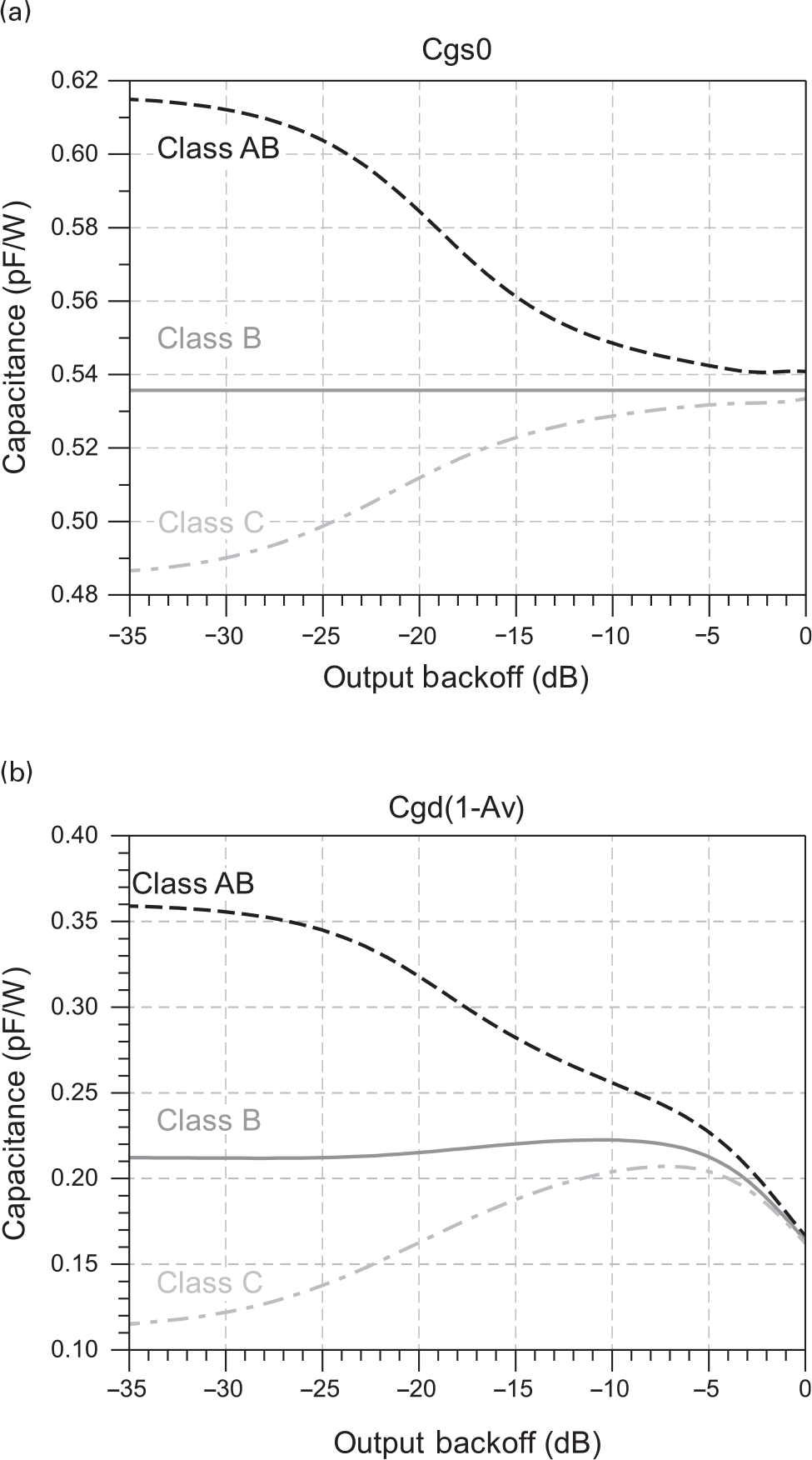
Figure 7.10 Normalized (per watt) profiles of (a) the Cgs0 component and (b) the input Miller reflected Cgd for a GaN HEMT based PA.
As far as the PA output node is concerned, since the voltage gain is normally very high, the output Miller reflected Cgd variation [Cgd(Av − 1)/Av] is almost negligible. Thus, the Cds variation will be the main contributor to the phase shift on the fundamental vDS voltage, according to equation (7.2).
 (7.2)
(7.2)The Cds0 capacitance variation for both Si LDMOS and GaN HEMT based PAs is depicted in Figure 7.11. Again, although the capacitance profile shapes of both devices are very similar, their values are completely different, with Cds0 being much higher for Si LDMOS based PAs. Actually, for GaN HEMT based PAs, the Cds0 variation is so small when compared with the input capacitance variation (see Figures 7.10 and 7.11) that it will be insignificant for the overall amplitude nonlinearity (AM/AM) or phase shift (AM/PM) of the PA.
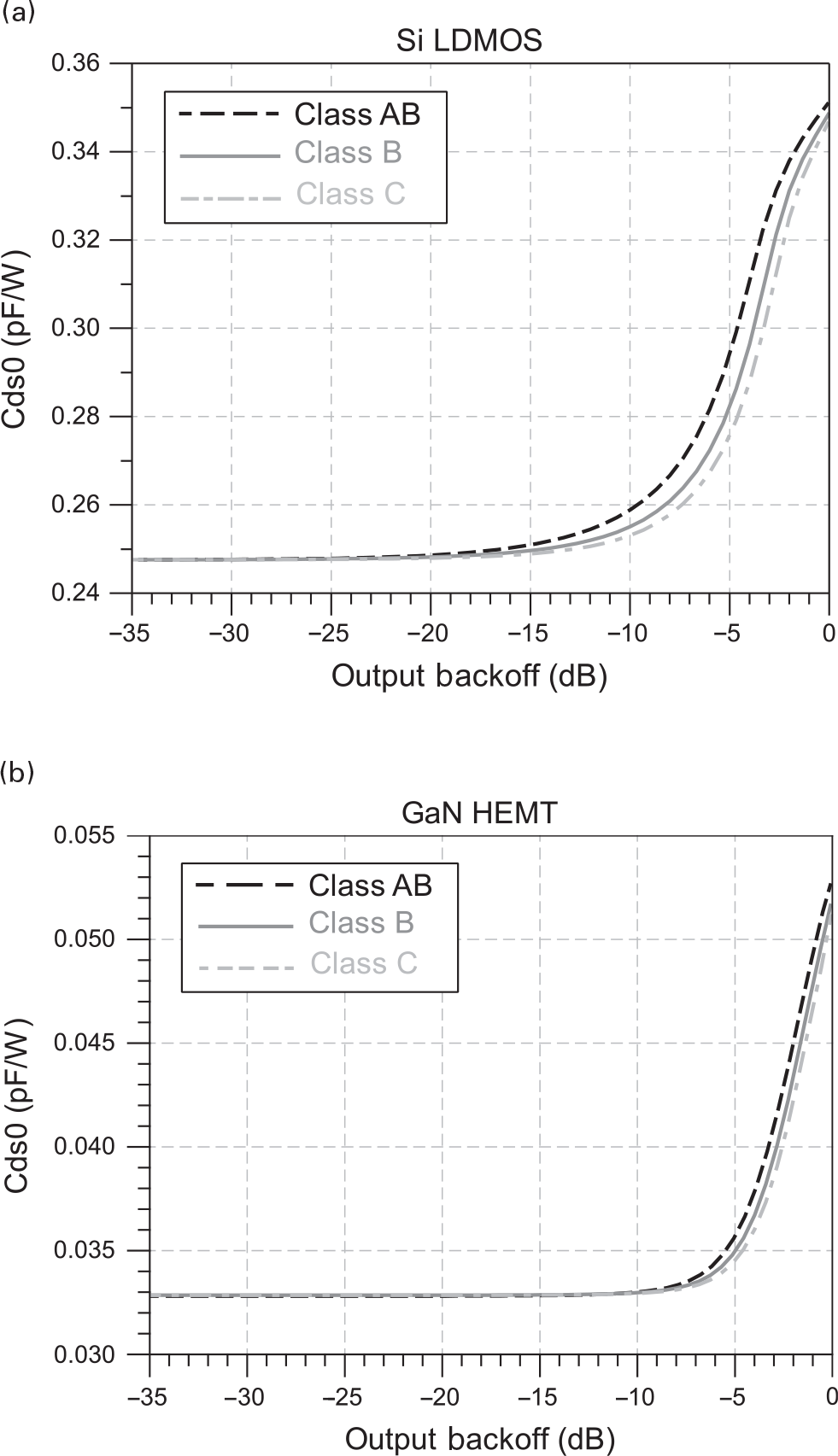
Figure 7.11 Normalized (per Watt) profiles of the Cds0 component of (a) Si LDMOS and (b) GaN HEMT based PAs.
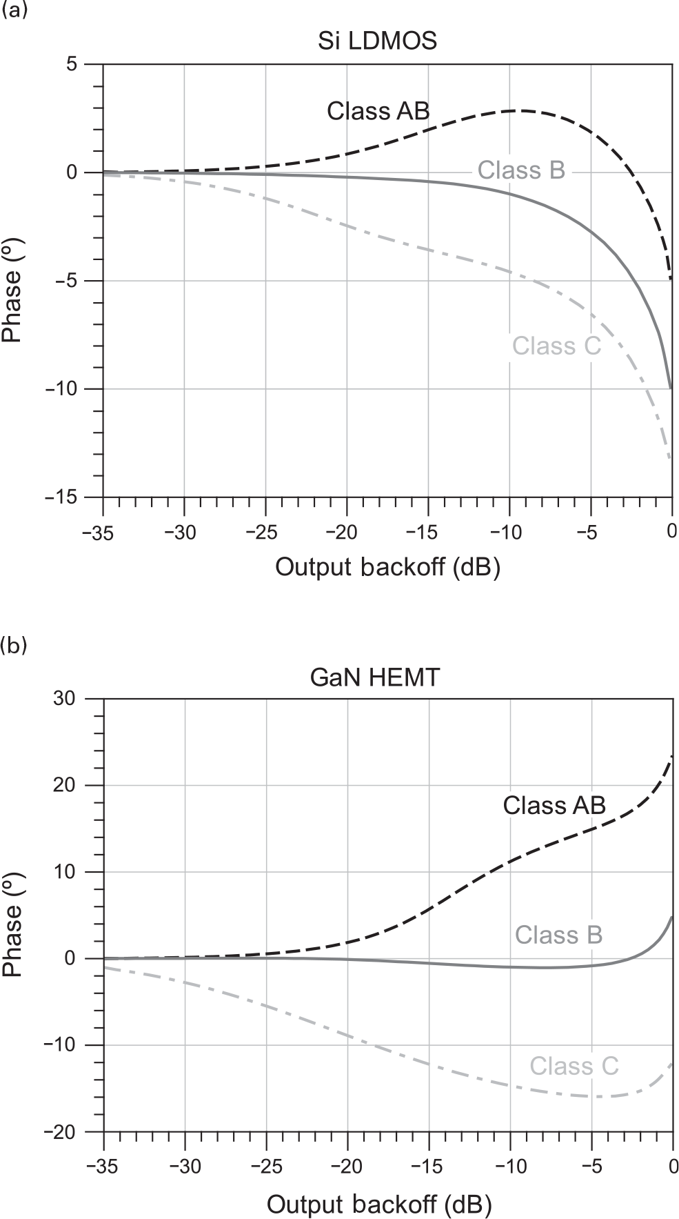
Because the iDS(vGS,vDS) nonlinearity is the dominant contributor to the PA amplitude, AM/AM, distortion, the main effect of capacitance nonlinearities is on the amplitude dependent phase shift, AM/PM. But, contrary to what happens with the iDS(vGS,vDS) nonlinearity, and thus with the amplitude distortion, these two technologies present quite different intrinsic capacitance variations. Hence, Si LDMOS and GaN HEMT based PAs evidence significantly distinct AM/PM characteristics, as shown in Figure 7.12. For Si LDMOS, the Cds0 variation is the major contributor to the AM/PM distortion, producing an almost phase-lagging behavior for all operation classes; only a slight phase-leading behavior is presented at the mid-power region for class AB due to the initial Cgs0 reduction. Conversely, the AM/PM distortion of GaN HEMT PAs is mostly determined by the phase shift imposed on the Vgs phasor voltage, due to Cgs0 and input Miller reflected Cgd variation. Therefore, since this capacitance variation is tied to the voltage gain, the AM/PM characteristic presents an opposite behavior to the AM/AM characteristic, as can be seen when we compare the AM/AM behavior shown in Figure 7.7 and the AM/PM of Figure 7.12(b).
7.1.4 Device Model Implementation in Commercial Microwave Circuit Simulation Platforms
To finalize this section devoted to illustrate the use of nonlinear models and computer-aided design tools in predicting the major RF characteristics of microwave devices, we now show how the above nonlinear models can be implemented in the available commercial simulators, such as the Keysight Technologies Advanced Design System, ADS [13], and the Applied Wave Research Microwave Office, MWO [14]. For that, we will use simple model formulations of the bidimensional nonlinear iDS(vGS,vDS) current and the assumed one-dimensional gate-source charge, Qgs(vGS), or capacitance, Cgs(vGS).
For the iDS(vGS,vDS) formulation we will use a model (7.3a) consisting in the product of (7.3b) and (7.3c), which describe the iDS dependence on the vGS and vDS voltages, respectively. Figure 7.13 shows the I/V curves of this simple model and the respective derivatives, Gm and Gds.
in which
 (7.3b)
and

Figure 7.13 (a) iDS(vGS,vDS), (b) Gm(vGS) and (c) Gds(vDS) profiles of the example formulae used to illustrate how to implement nonlinear static models in commercial nonlinear circuit simulators.
As far as the Qgs(vGS) formulation is concerned, we will adopt the model (7.4) – that we have used in the core of iDS(vGS) model (7.3b) – leading to the Cgs(vGS) hyperbolic tangent expression of (7.5). The profiles for these Qgs(vGS) and Cgs(vGS) models can be shown in Figure 7.14(a) and (b), respectively.
 (7.4)
(7.4)
Figure 7.14 (a) Qgs(vGS) and (b) Cgs(vGS) profiles of the model used to illustrate the implementation of nonlinear capacitance/charge models in commercial nonlinear circuit simulators.
The model implementation itself in ADS can be readily done with symbolically defined device, SDD, components. These components allow us to define the desired equations as a function of the voltages, currents, or their derivatives. Figure 7.15 illustrates the implementation of our Qgs(vGS) charge and iDS(vGS,vDS) current models.

Figure 7.15 Qgs(vGS) and iDS(vGS,vDS) model implementation in the ADS simulator with a symbolically defined device component.
To implement a model in MWO, we can use APLAC netlists. There, we define not only the charge and current equations, but also their derivatives to improve the simulator convergence. Tables 7.1 and 7.2 show the APLAC-MWO netlist implementation of our Qgs(vGS) and iDS(vGS,vDS) models, respectively. After implementation of these netlists, we need to compile and import them to a schematic, as is shown in Figure 7.16.
Table 7.1 Qgs(vGS) model implementation in the MWO with an APLAC netlist.
DefModel Cgs 2 n1 n2
+ PARAM 4 Cgs0 Acgs Vcgs Kcgs
Function vgs = CV(0)
Function Qgs_vgs {qv cv} [
+qv = (Cgs0*vgs + (Acgs*(vgs + Vcgs + ln(2*cosh(Kcgs*(vgs − Vcgs)))/Kcgs))/2);
+cv = (Cgs0 + 0.5*Acgs*(tanh(Kcgs*(vgs − Vcgs)) + 1));
+qv,
+cv]
VCCS CgsVccs n1 n2 1 n1 n2 Qgs_vgs C
EndModel
Table 7.2 iDS(vGS,vDS) model implementation in the MWO with an APLAC netlist.
DefModel Ids 4 n1 n2 n3 n4
+PARAM 13 Beta
Function vgs = CV(0)
Function vds = CV(1)
Function ids_vgs_vds {Fgs, Fds, dFgs_dvgs, dFds_dvds} [
+Fgs = (0.5*Beta/Kg)*(Kg*(vgs − VT) + ln(exp(Kg*(vgs − VT)) + exp(−Kg*(vgs − VT))));
+Fds = tanh(alfa*vds);
+dFgs_dvgs = 0.5*Beta*(1 + tanh(Kg*(vgs − VT)));
+dFds_dvds = alfa*(1 − tanh(alfa*vds)^2);
+Fgs*Fds,dFgs_dvgs*Fds,Fgs*dFds_dvds]
VCCS Idsvccs n3 n4 2 n1 n2 n3 n4 ids_vgs_vds
EndModel

Figure 7.16 Qgs(vGS) and iDS(vGS,vDS) schematic of the imported APLAC netlists in the MWO simulator.
7.2 Computer-Aided Power Amplifier Design Example
After having concluded our explanation of the impact of some of the active device model parameters in the performance of the circuits in which these devices operate, we will now move on to discuss a particular application example: a GaN HEMT based medium-power amplifier for mobile communications. For that, we will show how computer-aided design tools can help with the bias point and input and output termination selection and how they can help in the performance evaluation.
7.2.1 Bias Point Selection for High Efficiency
Starting the PA design flow with the bias point selection, we will use harmonic-balance (HB) simulation and our previously discussed GaN HEMT model to help us search for the quiescent point that presents the best compromise between efficiency and linearity.
For maximized output voltage excursion, and so linear output power capability, we consider a typical current mode design where vds(t) is assumed nearly sinusoidal, and the VDS quiescent point is selected as the middle point between the device’s knee and breakdown voltages, VK and VBR, or VDS = 28 V, as is recommended by the device’s manufacturer.
On the other hand, maximized efficiency requires a gate voltage VGS close to the threshold voltage, VT, which, in an idealized piecewise linear device, would correspond to class B operation with a flat gain. In a real FET, the VGS quiescent point that we should use to obtain a maximally flat gain is not well-defined, since the turn-on is not abrupt but smooth. However, we can still define it as the VGS quiescent point where small-signal input 3rd-order nonlinearity vanishes [15]. This could be thought of as the point of vanishing Gm3 ≡ ∂3iDS/∂vGS3 obtained from a small-signal two-tone test, or, alternatively, from small-signal harmonic distortion (see [15–17]) or of vanishing ∂2Gm/∂vGS2, i.e., the first inflection point of the transconductance, Gm(VGS), characteristic, derived from small-signal linear S-parameter data.
Unfortunately, this traditional methodology is not appropriate for our GaN HEMT as its small-signal VT is different from the actual large-signal VT, due to the different thermal and trapping states determined by the dc quiescent, and the large-signal operating points. To illustrate this, Figure 7.17(a) and (b) present two gain versus input power drive level characteristics respectively measured with a CW and with a two-tone signal whose period of the envelope is much smaller than the device’s time constants associated with its thermal or trapping phenomena. Although Figure 7.17(a) seems to correspond to a class B biased PA while Figure 7.17(b) to a PA biased in class C, they were measured on the same device with exactly the same dc quiescent point.

Figure 7.17 Gain versus input drive level of the same device and quiescent point, but driven with (a) a CW signal of increasing amplitude and (b) a two-tone signal of 1 kHz frequency separation. Note how the curve of (a) could misleadingly indicate a class B operation, while the one of (b) reveals a class C gain characteristic imposed by the trapping induced VT shift.
These two curves clearly reveal the threshold voltage shift caused by the trapping effects of GaN HEMTs [18]. At low drive levels, the vDS peak voltage is not much different from the VDD bias and the associated drain-lag traps are charged to their reference level. The threshold voltage is also at its reference level, VT0, and VGS ≈ VT0 is such that the device shows a typical flat small-signal gain class B behavior. However, when the drive level increases, the new vDS peak voltage sets these traps to a different state, increasing VT to VT1, so that, now, the device is no longer biased at VGS ≈ VT1 but at VGS < VT1, i.e., in class C. If now the drive level is decreased so slowly that the trap state dynamics can follow the decrease of vDS peak voltage, the device will show again its flat small-signal gain, as seen in Figure 7.17(a). If, on the other hand, this decrease is much faster than the traps’ discharging time, the device will keep its apparent class C bias, exhibiting an increasing small-signal gain as shown in Figure 7.17(b).
Therefore, a different strategy has to be adopted. Instead of the usual sinusoidal HB simulations, which mimic the CW lab tests, two-tone harmonic-balance (or envelope transient harmonic-balance, ETHB) simulations were used to determine the VGS quiescent point of best efficiency-linearity trade-off. This is what is shown in Figure 7.18(a) in terms of power added efficiency, PAE, Figure 7.18(b) gain, Gain, and 7.18(c) carrier-to-intermodulation-ratio, IMR, for three different VGS biases corresponding to shallow class AB, class B and shallow class C operation.

Figure 7.18 Two-tone harmonic-balance simulations of (a) power-added efficiency, PAE, (b) gain, Gain, and (c) carrier-to-intermodulation-ratio, IMR, versus input drive level for three different VGS quiescent points (VGS = −3.3 V, VGS = −3.58 V and VGS = −3.9 V) corresponding to shallow class AB, class B and shallow class C operation, respectively.
Since the simulated results indicate similar values of PAE but considerably different ones for IMR and gain profile flatness, the class B bias point of VGS = −3.58 V was selected.
7.2.2 Source- and Load-Pull Simulations
After having selected a convenient quiescent point for the best trade-off between efficiency and linearity, we will now select proper source and load terminations.
Again, this will be done using the circuit simulator, avoiding the need for tedious source/load-pull measurements and expensive equipment. Actually, if good models are available (which is not necessarily the case when dealing with very high power devices), we have an advantage in the simulator over what we can do in the lab. Indeed, having access to the intrinsic device’s voltages and currents (something particularly useful in prematched FETs), we can simulate source/load-pull with ideal lossless components directly at very low impedances, i.e., without the need to use impedance transformers to convert them to the normalized 50 Ω found in the real lab. Furthermore, with a good model, we may even start by calculating a first estimate of the required load.
7.2.2.1 Estimation of the PA Required Load
In order to obtain a first estimate of the PA required load, we will use the Cripps load-line method [1] for the intrinsic load resistance that maximizes linear output power capability (from now on designated as the power load, RL_pwr or ZL_pwr) and its extension to optimum efficiency provided by [2] (which we will designate the efficiency load, RL_eff or ZL_eff). We need to start by drawing the intrinsic iDS(vGS,vDS) output curves. However, what we would obtain from a typical dc simulation would be the curves of Figure 7.19(a), which suffer from thermal and trapping phenomena. To overcome this, we need to first set the temperature and the trap states at values close to the ones we expect the amplifier to operate in steady-state, and then dynamically test the device from that quiescent state.

Figure 7.19 (a) Conventional dc I/V curves obtained from a dc simulation and (b) pulsed I/V curves simulated via a transient analysis in which the quiescent point was set at VDS = vDS_Max and VGS < VT, whose pulse duration was significantly smaller than the device’s thermal and de-trapping time-constants and the duty cycle was 0.1%. (c) Comparison between the dc and pulsed IDS versus VGS for a VDS = 28 V to show the shift in the threshold voltage due to trapping and thermal effects.
From the device’s datasheet, such a device, driven by a WiMAX signal, is supposed to deliver about 2 W of average power with 26% of drain efficiency. So, since its thermal resistance is on the order of 8 K/W [19], we obtain a rough estimate of 46ºC of temperature increase over room temperature. Hence, we set the device model temperature control node to 71ºC. As far as the trap states are concerned, we will assume that they will be imposed by the maximum vDS voltage, and that this value is given by: vDS_Max = VDS + (VDS − VK)≈51 V. Consequently, the I/V curves we are interested in are the ones obtained from a transient pulsed I/V simulation in which the quiescent point is set at VDS = vDS_Max and VGS < VT, whose pulse duration is significantly smaller than the device’s thermal and detrapping time-constants and the duty cycle is some 0.1% or lower. Figure 7.19(b) depicts the output I/V curves obtained from such a transient pulsed I/V simulation.
Superimposed to these pulsed I/V curves is the ideal class B dynamic load line, the selected quiescent point, Q, and its correspondent position after the discussed shift determined by the thermal and trap steady-states. According to the Cripps load-line method, such a dynamic trajectory requires an intrinsic termination of RL_pwr = 19 Ω, which, transformed by the device’s output parasitic network, leads to a fundamental termination of ZL_pwr = 14.4 − j7.2 Ω at the device’s drain terminal.
As far as the optimum intrinsic termination for maximized drain efficiency is concerned, the approximate estimate of [2] led to an RL_eff = 79 Ω and a corresponding extrinsic termination of ZL_eff = 72.9 + j15 Ω.
7.2.2.2 Simulated Load-Pull Contours
Although these two ZL values could already be used to get an estimate of a fundamental load impedance capable of providing a good compromise between output power capability and efficiency, a set of CW HB simulations produced the load-pull contours shown in Figure 7.20. Commercial nonlinear microwave circuit simulators already include preprogrammed aids to perform automatic load-pull simulations as shown in Figure 7.20(b) given a set of predefined test loads distributed as in Figure 7.20(a). As a matter of fact, such a simulation requires also the definition of a particular source impedance (we selected one that could produce a reasonable input match for the maximum output power load) and load and source impedances at all harmonics. In the present case, we selected a short circuit at all even and odd harmonics, as is the condition required for current-mode class B operation.

Figure 7.20 (a) Set of predefined load impedances used to simulate the output power (dashed lines) – PMax = 43.1 dBm and PStep = 0.5 dB – and drain efficiency (solid lines) – ηMax = 76.6% and ηStep = 5% – load-pull contours shown in (b).
These conditions led to a maximum output power of 43 dBm (about 20 W), a maximum drain efficiency of 76% and to an optimum load of ZL_opt = 29.3 − j3.3 Ω, which represents a good compromise between these maximum output power and efficiency figures. Such a load provides an output power of 41 dBm (12.6 W) and a drain efficiency of 74%.
An alternative to the current-mode class B harmonic termination set previously used could also be chosen. Specifically, we now use the set determining class F operation, i.e., a short circuit to all intrinsic even order harmonics and an open circuit to all odd order ones. In this case, the obtained load-pull contours are the ones shown in Figure 7.21, from which a maximum power of nearly 43.5 dBm (22.4 W) and maximum efficiency of 93% are predicted. As shown in Figure 7.21, the optimum compromise between output power and efficiency now corresponds to an improved output power of 42.5 dBm (22.6 W) and efficiency of 89%, reason why this was the adopted configuration.

Figure 7.21 Output power (dashed lines) – PMax = 43.5 dBm and PStep = 0.5 dB – and drain efficiency (solid lines) – ηMax = 93% and ηStep = 5% – load-pull contours obtained when the harmonic terminations were selected to determine a class F operation and the set of tested loads were again the ones shown in Figure 7.20(a).
The dynamic load-line and the intrinsic voltage and current waveforms shown in Figure 7.22 (a) and (b), respectively, confirm the expected class F operation.

Figure 7.22 (a) Dynamic load-line and (b) intrinsic vDS(t) (—) and iDS(t) (…) waveforms of the device terminated for class F operation.
7.2.2.3 Small- and Large-Signal Stability Check
Before selecting the source impedance, a stability check (both at the dc operating point and the large-signal nominal excitation amplitude) was conducted and, as shown in Figure 7.23(a), it was verified that the selected load impedance was dangerously close to the region that produces a negative input resistance (|Γin| > 1, indicating a potentially unstable design). Therefore, following the advice of the GaN HEMT manufacturer, a stabilizing resistor of 5 Ω was introduced in series with the gate terminal, resulting in the new stability region shown in Figure 7.23(b).

Figure 7.23 (a) Load terminations of negative input resistance (|ΓIN| > 1) simulated at the large-signal excitation amplitude, and the selected load termination, which shows that such a design is too close to instability. (b) Same simulation but now when the device includes a 5 Ω stabilizing resistor at the gate terminal.
To be complete, such a stability check would have to be done at all possible excitation amplitudes, with the aid of a small-signal perturbation of the LSOPs, and extended to all frequencies at which the device is active, something that is theoretically complicated, and quite cumbersome in practice. Alternatively, a single stability check may be performed with the aid of a transient simulator. Nevertheless, one would still need to repeat this transient simulation for, at least, the cases of infinitesimal and nominal excitation levels.
7.2.2.4 Simulated Source-Pull Contours
With the selected impedance for the fundamental, and the other ideal source and load harmonic terminations for class F operation, we then conducted a source-pull for the fundamental resulting in the contours of Figure 7.24. From these, a maximum output power of 42.5 dBm (17.8 W) and a maximum efficiency of 85.6%, were obtained for the source impedance of ZS = 7.6 + j11.9 Ω.

Figure 7.24 Simulated source-pull contours of output power (dashed lines) – PMax = 42.5 dBm and PStep = 0.5 dB – and efficiency (solid lines) – ηMax = 85.6% and ηStep = 5% –, for constant source available power equal to 24 dBm, when the device is terminated at the output to guarantee optimum class F operation.
After several iterations of source and load tuning, the found source and load terminations were the ones listed in Table 7.3.
| Source impedances | Load impedances |
|---|---|
| ZS(f0) = 7.6 + j11.9 Ω | ZL(f0) = 27 + j3.4 Ω |
| ZS(2f0) = −j8.3 Ω | ZL(2f0) = −j14.5 Ω |
| ZS(3f0) = −j12.6 Ω | ZL(3f0) = +j69.6 Ω |
Note that, because of the transistor package parasitics and the design of the matching networks, only the first three harmonics could be considered, which led to a predicted design performance of 42 dBm (15.8 W) of output power and 81.8% of efficiency.
7.2.3 Input and Output Bias and Matching Network Design
Having selected the input and output termination impedances, initial matching and biasing networks were designed. This process started by using ideal transmission line elements, which were then converted into microstrip elements. This led to a first draft of the layout, which was then retuned, representing these planar structures by S-parameter matrices obtained from an electromagnetic simulator. Such a tuning process should be made for both the desired frequency response around the carrier and harmonics as well as around dc, since this determines the so-called video-bandwidth, the main characteristic responsible for the amplifier’s envelope memory effects. This electromagnetic simulation of the microstrip layout is particularly important for high-power devices that usually require transmission lines of very low characteristic impedance. In this scenario, the obtained layout tends to have microstrip lines or discontinuities (such as microstrip steps, T and cross junctions, bends, etc.) whose geometrical dimensions may fall outside of the validity of the simulator’s embedded microstrip element models.
After this layout design process, the result was the one shown in Figure 7.25.

7.2.4 Performance Evaluation
After the use of the described nonlinear simulating techniques for a typical circuit design, we will now illustrate the utilization of these tools in the context of performance evaluation. For that, we will make a set of measurements of our PA, to compare with results obtained from the nonlinear circuit simulator.
Because of the specific responses a nonlinear circuit offers to distinct excitations, the illustrated measurements and simulations will be grouped according to the tested class of stimuli. Therefore, as is quite usual in the test of PAs, these classes of excitations will be a CW signal and a modulated carrier. However, contrary to the CW simulations, which are quite straightforward, that is not the case of the simulations conducted with the modulated stimuli because the time-domain description of the aperiodic modulation requires that every component (even the EM simulated blocks of the matching networks) is represented by an appropriate lumped equivalent circuit, e.g., a broadband spice model, BBSM [4]. So, before we proceed to simulate the circuit driven by a modulated signal with, e.g., envelope transient harmonic-balance, ETHB, it is always advisable to test the generated equivalent circuit models comparing HB responses of the circuit with similar results obtained via ETHB. This requires a test whose results can be obtained from both HB and ETHB, like periodic multitone excitations.
7.2.4.1 Continuous-Wave Testing
Continuous-wave measurements and simulations are the simplest tests we can make in our circuit because most RF instrumentation and simulators were especially conceived for that purpose. These tests have been grouped into linear and nonliner measurements, according to the considered excitation amplitude and required instrumentation or simulation tools. However, since the circuit’s small-signal response should naturally arise in the limit of the large-signal tests when the excitation amplitude is sufficiently small (so as not to generate harmonics or change the dc quiescent point), we will treat them in a unified manner. Hence, we will place the PA in a matched source and load environment and then sweep the excitation amplitude, from small signal up to a few dB of gain compression, and measure the input–output transfer characteristic in amplitude and phase. These amplitude and phase profiles are known as the quasi-static AM/AM and the AM/PM and are shown in Figure 7.26(a) and (b).

If these tests were accompanied by measuring the input, output, and dc supplied powers, an efficiency versus drive level plot like the one shown in Figure 7.27 could also be reproduced.

Figure 7.27 Measured and HB simulated power-added-efficiency of the tested PA circuit for the selected bias (VGS = −3.58 V).
7.2.4.2 Multitone Testing
As said in the introduction to this section, multitone testing constitutes a performance evaluation procedure, but it also serves as a means to test the accuracy of the equivalent circuit models used in the envelope following simulators that operate in the time domain. This is the reason why two-tone and four-tone tests will be treated in this section, and their measurement results compared with multitone harmonic-balance and envelope transient harmonic-balance simulations.
Starting with two-tone tests, Figure 7.28 is a repetition of the AM/AM plots discussed above for the CW excitation but now measured capturing the envelope time evolution (with a vector signal generator and a vector signal analyzer instead of a network analyzer) for a two-tone stimulus of constant frequency separation (Δf = 50 kHz) and increasing peak power level.

Figure 7.28 Dynamic gain (or dynamic AM/AM) profiles of our PA example obtained with two-tone tests of constant frequency separation (Δf = 50 kHz) and increasing peak envelope power level: (a) measurements and (b) two-tone HB simulated results.
Note the progressive reduction of small-signal gain verified for the increasing vDS(t) voltage peak, an indication of the GaN HEMT long-term memory effects [18].
Figure 7.29 describes another set of two-tone tests, but now with a constant input peak envelope power (PEP = 24.7 dBm) and increasing separation frequency to evidence the PA’s long-term dynamic behavior.

Figure 7.29 Dynamic gain (or dynamic AM/AM) profiles of our PA example obtained with two-tone tests of constant input peak envelope power level (PEP = 24.7 dBm) and increasing frequency separation (a) measurements and (b) two-tone HB simulated results.
To close this discussion regarding two-tone tests, Figure 7.30 is an illustrative spectrum of the measured and simulated results obtained for the input PEP of 24.7 dBm and a separation frequency of 0.8 MHz.

Figure 7.30 Illustrative measurements and HB simulated results of a two-tone test performed with an input PEP of 24.7 dBm and a separation frequency of 0.8 MHz.
Finally, Figures 7.31 and 7.32 summarize the measurement and simulation tests conducted with a 4-tone excitation in order to check the accuracy of the time-domain envelope simulation models. These figures compare the dynamic AM/AM and AM/PM profiles (Figure 7.31) and spectra (Figure 7.32) obtained with measurements, multitone HB simulation and ETHB envelope following simulation at the same conditions.

Figure 7.31 (a) Dynamic AM/AM and (b) AM/PM profiles directly obtained from laboratory measurements and multitone HB and ETHB simulations of our PA circuit example excited with a 4-tone stimulus.

Figure 7.32 Measured and simulated (with both HB and ETHB) spectra corresponding to the 4-tone tests reported in figure Figure 7.31.
7.2.4.3 Modulated Signal Testing
As a final example of the nonlinear measurement and simulation tests on our PA circuit example, we excited it with a 64-QAM signal of 24.1 dBm of available input peak envelope power and 10 MHz of bandwidth. Figure 7.33–7.35 describe the obtained results in several different forms.

Figure 7.33 (a) Dynamic AM/AM and (b) AM/PM profiles directly obtained from laboratory measurements and ETHB simulations of our PA circuit example excited with a 64-QAM signal of 10 MHz bandwidth.

Figure 7.34 Measured and ETHB simulated spectra corresponding to the time-domain dynamic AM/AM and AM/PM plots shown in figure Figure 7.33.

Figure 7.35 System-level constellation diagram obtained from the ETHB simulations reported in Figures 7.33 and 7.34.
Similarly to what was done before, Figures 7.33 and 7.34 report the measured and ETHB simulated time-domain AM/AM and AM/PM and corresponding frequency-domain spectra, respectively.
As a final illustration of presently available nonlinear simulation capabilities, Figure 7.35 depicts a system level constellation diagram of the PA response to the 64-QAM signal, from which error vector magnitude, EVM, performance figures could be drawn.
7.3 Summary
The authors hope that this closing chapter provided an illustration of some of the concepts addressed in the book’s preceding parts, putting them in an application context, so that their significance in nonlinear microwave circuit design can be better understood.
We started by revisiting some features of the active device modeling presented in the previous chapters discussing their impact on the predicted circuit behavior. Then, a step-by-step design and verification procedure for a wireless medium-power amplifier based on a GaN HEMT device was presented. This exemplified how a nonlinear device model, connected to some commercial nonlinear simulation tools, can be used to aid, first, the design and, then the test of the selected circuit.
This way, we showed how these modeling and simulation techniques can lead to a more profound understanding of the circuit operation, and thus to an optimized circuit design. The consequent reduction in the number of iterations necessary for the circuit design/implementation justifies the effort spent on device characterization and modeling.
Actually, the modeling and simulation techniques addressed in this book, and experimented in this last chapter, have become indispensable in modern nonlinear microwave circuit designs, enabling monolithic implementations, higher operating frequencies, wider bandwidths, or architectures of increased levels of complexity.
References
 Findit@CUHK Library | Google Scholar
 Findit@CUHK Library | Google Scholar
 Findit@CUHK Library | Google Scholar
 Findit@CUHK Library | Google Scholar
 Findit@CUHK Library | Google Scholar
 Findit@CUHK Library | Google Scholar
 Findit@CUHK Library | Google Scholar
 Findit@CUHK Library | Google Scholar
 Findit@CUHK Library | Google Scholar
 Findit@CUHK Library | Google Scholar
 Findit@CUHK Library | Google Scholar
 Findit@CUHK Library | Google Scholar
 Findit@CUHK Library | Google Scholar
 Findit@CUHK Library | Google Scholar
 Findit@CUHK Library | Google Scholar
 Findit@CUHK Library | Google Scholar
 Findit@CUHK Library | Google Scholar
 Findit@CUHK Library | Google Scholar
 Findit@CUHK Library | Google Scholar