6.1 Introduction
This chapter presents a survey of selected foundations and principles of large-signal device modeling for nonlinear circuit simulation. The chapter begins by recalling the early connection between simple transistor physics and nonlinear circuit theory. The evolution from simple physically based models to empirical models of various types is outlined, including table-based models and modern techniques based on artificial neural networks (ANNs). Formal as well as practical considerations related to ensuring robust model nonlinear constitutive relations for currents and charges are illustrated throughout. The relationship of large-signal models to linear data is treated extensively, for the purpose of proper parameter extraction and also for investigating the conditions under which bias-dependent small-signal data can be integrated to infer large-signal constitutive relations. Quasi-static models are analyzed in detail, and their consequences are deduced and checked against experimental device data.
Terminal charge conservation modeling concepts are considered in detail, including a treatment of charge modeling in terms of both depletion and “drift charge” components. Concepts of stored energy related to charge modeling are introduced including presently unresolved issues requiring future research.
Models for dynamic physical phenomena, especially self-heating and trapping mechanisms for III-V FETs, are introduced to explain the measured device behavior and to illustrate the reasons that quasi-static models are inadequate for most transistors. Symmetry principles are presented formally and as a practical tool to help the modeler ensure that the mathematical device model is consistent with the physical device properties.
Several modern modeling applications of nonlinear vector network analyzer (NVNA) data are presented. Even for simple models, the benefits of NVNA data, for parameter extraction and easy model validation at the time of extraction, offer large gains in modeling flow efficiency. For models incorporating multiple dynamic phenomena, such data can be used to efficiently separate and identify the independent effects. As an example, NVNA waveform data are used to generate a detailed nonlinear time-domain simulation model for III-V FETs, taking advantage of direct identification techniques for dynamical variables and the power of ANNs to fit scattered data in a multidimensional space. The model features dynamic self-heating and charge capture and emission mechanisms, and is extensively validated for several GaAs and GaN transistors.
The restriction to linear model behavior covered in Chapter 5 is removed, and therefore the economy of description afforded by the frequency domain treatment of Chapter 5 disappears. The models discussed in this chapter are lumped, meaning that their constitutive relations are defined via nonlinear current-voltage and charge-voltage relations, expressed in the time-domain. Lumped models are appropriate for transistors for excitation frequencies up to approximately the cutoff frequency, fT, beyond which the devices become more and more distributed. Since the useful range of transistor applications is usually below fT, we limit ourselves to the lumped nonlinear description.
6.2 Transistor Models: Types and Characteristics
6.2.1 Physically Based Transistor Models
The physics of semiconductor devices involves a complicated combination of quantum mechanics, solid state physics, material science, electromagnetism, and nonequilibrium thermodynamics. In the early 1950s, William Shockley derived the time-dependent terminal currents at the drain and gate of a field-effect transistor (FET) starting from the Poisson and current continuity partial differential equations [1]. The explicit solutions are shown in (6.1)–(6.4). Shockley made several simplifying assumptions along the way, such as field-independent charge carrier mobility (constant μμ), the gradual channel approximation (the electric field is primarily perpendicular to the active channel), and neglecting the effects of self-heating. A simple derivation can be found in [2] (see also [3]).
 (6.1)
(6.1)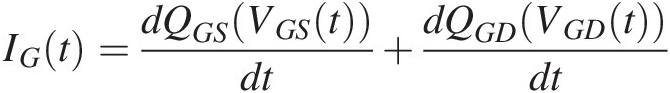 (6.2)
(6.2) (6.3)
(6.3) (6.4)
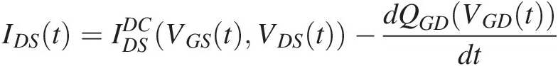
(6.4)Here WtotWtot is the total gate width, LL is the gate length, aa is the channel depth, qq is the magnitude of the electron charge, εε is the dielectric constant of the semiconductor, NDND is the doping density of the semiconductor (assumed uniform), and ϕϕ is the built-in potential. The time-dependent drain and gate currents, (6.1) and (6.2), are evidently decomposable into distinct contributions from a voltage-controlled current source and two nonlinear two-terminal charge-based capacitors. That is, the solution of the physical partial differential equations leads to a rigorous representation, at the device terminals, in terms of standard lumped nonlinear circuit theory.
The nonlinear equivalent circuit corresponding to (6.1) and (6.2) is given in Figure 6.1. The functional forms (explicit nonlinear functions) of the constitutive relations for the current and charge sources are given by the expressions (6.3) and (6.4).
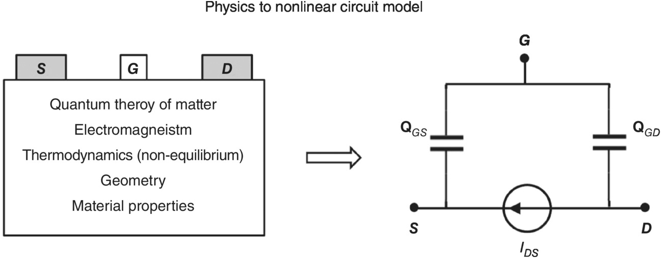
Figure 6.1 Physics to circuit representation.
While the equivalent circuit of Figure 6.1 is usually justified based on its “resemblance” to the physical structure of the device (see also Figure 5.1), the above discussion provides a deeper explanation and justification. Moreover, in addition to the topology of the equivalent circuit, the details of the constitutive relations are obtained from this analysis.
The electrical performance of any circuit designed using the FET, in combination with other electrical components, can therefore be simulated by solving the set of ordinary nonlinear differential equations of circuit theory, using the methods of Chapter 2, rather than the partial differential equations of physics. In a very important sense, the nonlinear equivalent circuit representation of the transistor is a behavioral model suitable for efficient simulation of components and circuits at higher complexity levels of the design hierarchy [4]. This is quite fortunate, since it is not at all practical to solve the detailed partial differential equations of physics, at the transistor level, for a circuit composed of many transistors.
The constitutive relations, the particular functions for the I–V and Q–V relations (6.3) and (6.4), are closed-form nonlinear expressions involving the controlling terminal voltages, VGSVGS and VGDVGD, for the FET. We point out here that the domain of voltages over which these constitutive relations are defined is limited to 0 ≤ VDS ≤ VDSsat0≤VDS≤VDSsat where VDSsat=qNDa22ε−ϕ−VGS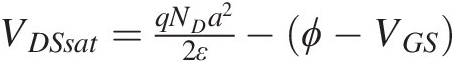 . At VDS = VDSsatVDS=VDSsat, the channel is pinched off and the slope of the I–V curve (the output conductance) is zero. This condition also determines the threshold voltage, VTVT, as that value of VGSVGS required to pinch off the channel when the drain-source voltage is zero. We have VT=ϕ−qNDa22ε
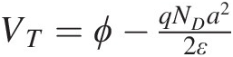 .
.
The domain of the model can be extended by defining the channel current to be constant, at the value IDS(VGS, VDSsat)IDSVGSVDSsat, for values of VDS>VDSsatVDS>VDSsat. The terminal voltages, VGSVGS and VGDVGD, are also limited to values less than the built-in potential, ϕϕ, at which the constitutive relations would become singular.
The notion that a model, well-defined initially in a limited domain, must have its domain properly extended for robust simulation, is a common and important consideration for successful nonlinear device modeling. We will discuss this in more detail in Section 6.2.5.3.
An important benefit of good physically based models is that the parameters entering the nonlinear constitutive relations tend to be meaningful. This is true for the Shockley model, where parameters include physical constants (e.g., q, the electron charge magnitude) and geometrical dimensions of the device (e.g., the gate width, W, the gate length, L, and the channel depth, a). There are material properties such as εε, the dielectric constant of the semiconductor, and the mobility µ, of the charge carriers. Also entering the constitutive relations is the device design parameter, ND, the doping density of the semiconductor. Another important feature of the Shockley model, shared by many physically based models, is that the same parameters that enter the I–V constitutive relation (6.3) also enter the Q–V constitutive relations (6.4), coherently linking the resistive and reactive parts of the model through the common underlying physics.
A characteristic of the current-voltage constitutive relation (6.3) for the channel current is that it is a fully two-dimensional function that can’t be de-composed into a product of two one-dimensional functions. That is, generally speaking, we have the condition expressed by (6.5).
On the other hand, transistor technology has evolved rapidly since Shockley’s analysis. The basic physical assumptions that led to (6.3) and (6.4) no longer apply, and it is generally not possible to arrive at simple closed form expressions for the current and charges as functions of the controlling voltages. Ironically, due to the phenomenon of charge-carrier velocity saturation (beyond the Shockley theory based on constant mobility), expressions like (6.5) can be more accurate for modern FET devices than the Shockley model suggests. Indeed, for simplicity of analysis, the approximation IDS(VGS, VDS)≈g(VGS) ⋅ f(VDS)IDSVGSVDS≈gVGS⋅fVDS is used in the design example of Chapter 7.
Physically based models are predictive as long as the particular transistor technology is consistent with the physical assumptions. For example, where the Shockley model applies, the doping density could be changed and the resulting device characteristics would follow from (6.3) and (6.4) just by changing the numerical value for ND. Of course this also means device technologies based on different principles of operation require distinct physical models, even within the same class of transistors (e.g. FETs). For example, a Si MOSFET and a GaAs pHEMT will have different physical models, despite some semi-quantitative similarity in their measured performance characteristics.
6.2.1.1 Limitations of Physically Based Models
Classical physically based models may neglect (intentionally or otherwise) certain physics that can influence the actual DUT performance. A closed-form expression may not exist for the constitutive relations without further approximations that may render the model insufficiently accurate for circuit design. The detailed physics of new technologies may not be fully known when the technologies come on line. This means physically based models, robustly implemented in commercial simulators, may not be available for the latest device technologies when the transistors themselves become useful for practical designs and products. It often takes years for the development and implementation of a good physically based nonlinear simulation model for a new semiconductor technology that is itself continuing to evolve. Some physical models may require knowledge of parameters, such as trap energy distributions, that may not be knowable or extractable from simple measurements, thus reducing much of the practical utility for these types of models.
6.2.1.2 Brief Note on Modern Physically Based Transistor Models
Over the past decade, physically based transistor models have made a comeback with the advent of surface potential models, primarily for MOSFET technologies [5–7]. These models define nonlinear constitutive relations for the terminal voltages in terms of the surface potential and also the currents as functions of the surface potential. Together, these equations define, implicitly, the current-voltage and charge-voltage relationships. This is in contrast to defining the currents and charges explicitly as functions of the voltages. More recently, the surface potential approach has been applied to III-V FET technologies (e.g. GaN) [8]. Other modern physically based III-V FET models, such as that proposed in [9], are based on different approaches. We will not delve into the important topic of modern physically based RF and microwave transistor models any further here but mention that this could be a re-emerging and important future trend.
6.2.2 Empirical Models
To deal with the limitations of physically based models discussed in Section 6.2.1.1, so-called empirical models were introduced [10–17] and still play a dominant role in microwave and RF nonlinear design applications, especially in the III-V semiconductor systems (e.g., GaAs, GaN, and InP).
Empirical models assume that the same equivalent circuit topology, suggested by basic physical considerations, is capable of representing the device dynamic characteristics, but that the I–V and Q–V constitutive relations can be treated as generic and independent functions to be chosen based on simple measurements and ease of parameter extraction.
For example, a classical empirical FET model due to Curtice [17] defines constitutive relations by equations (6.6)–(6.9) for the same equivalent circuit as shown in Figure 6.1.
 (6.7)
(6.7)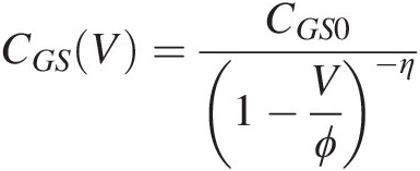 (6.8)
(6.8)For our purposes, V1V1, in (6.6), can be taken to be the gate-source voltage, VGSVGS, and V2V2 the drain-source voltage, VDSVDS.1 Contrary to the general case, (6.5), and neglecting the VDS-dependence of V1, the channel current (6.6) takes the form of a product of two univariate functions. The polynomial dependence on V1V1 is chosen for convenience. The corresponding parameters, A0 − A3A0−A3 have no physical significance. The parameter, γγ, is related to the voltage at which velocity saturation becomes important – a phenomenon not taken into account by the Shockley theory.
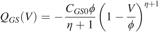
To simulate with the model, numerical values must be specified for each of the model parameters in all of the constitutive relations (6.6)–(6.9), typically by relating them to measurements on a reference device. This is the goal of parameter extraction. Obviously, the specific form of the intrinsic model constitutive relations can influence the parameter extraction strategy – the methodology by which the parameters are assigned numerical values. For the above model, {An}An define the gate-voltage dependence of the channel current, γγ determines where the I–V curves saturate with drain bias, and CGS0, CGD0, ϕ, and ηCGS0,CGD0,ϕ,andη are parameters determining the charge variation of the two capacitors as functions of their respective controlling voltages.
It is also clear from (6.6)–(6.9), that the channel current and charge storage (nonlinear capacitance) model are less strongly coupled to one another in this model than in the Shockley model. In particular, the built-in potential, ϕϕ, does not even enter the channel current constitutive relation, while it plays a determinant role in the input capacitance model for CGSCGS.
Equation (6.7) is a standard physically based bias-dependent junction model, with corresponding capacitance value given by (6.8) with typical parameter values in the range 0 < ϕ < 1, 0 < η ≤ 0.50<ϕ<1,0<η≤0.5. Equation (6.9) describes a capacitance with a fixed value independent of bias. Notice that despite having a symmetric equivalent circuit topology, Figure 6.1, the different functional forms for QGS(V)QGSV and QGD(V)QGDV makes the Curtice model quite asymmetric with respect to the source and drain. Compare this to the fully drain-source symmetric Shockley charge model where the two nonlinear capacitors have the same Q–V functional form given by (6.4). The significance of these statements will be discussed in the context of symmetry principles and their consequences, presented in Section 6.5.
6.2.3 Quasi-Static Models
Both the Shockley model of (6.1)–(6.4) and Curtice model of (6.6)–(6.9) are quasi-static models. That is, the constitutive relations depend only on the instantaneous values of the controlling variables (voltages in this case). There is no explicit time or frequency dependence in the relationships. This means, for example, that the IDSIDS current source will respond, instantaneously, to the applied intrinsic voltages, no matter how quickly the voltages may change with time. Similarly, the charge functions will respond, instantaneously, to the time-dependent applied intrinsic voltages.
An important consequence of a true quasi-static model, be it empirical or physically based, is that the resistive part of the intrinsic high-frequency RF and microwave model is fully determined and follows completely from the DC model characteristics. However, in real RF and microwave applications, the physical transistor is almost never operated in a true quasi-static condition. The RF signal is almost always much faster than the important thermal dynamic response, something we have not yet considered. For FETs, we will examine electro-thermal modeling in Section 6.6.
6.2.4 Empirical Models and Parameter Extraction
Since the constitutive relations of empirical models are chosen to fit the data, any deficiency of fit – at least for the I–V model fit to DC data – can be rectified by increasing the complexity of the function. For example, higher order polynomial terms can be added to the Curtice model IDSIDS constitutive relation (6.6). A problem with this approach, however, is that whenever the constitutive relations are changed, the parameter extraction process may also need to be modified.
Additionally, errors in the measurements will generally affect the model, since the parameter extraction process usually finds the best fit to the experimental data. The reader may wish to review, at this point, the more detailed discussion in Chapter 1, Section 1.5.1 about fitting static transfer functions.
For microwave FET devices of various types, several empirical models, notably the EEFET model family [14] and the Angelov (Chalmers) model family [15] and [16] are popular. The latter has evolved over 20 years to include many important dynamic effects such as self-heating and other dispersive or non-quasi static effects.
6.2.5 Nonlinear Model Constitutive Relations
6.2.5.1 Good Parameter Extraction Requires Proper Constitutive Relations
Even a simple intrinsic model constitutive relation, like that of Eq. (6.6), can be extracted improperly leading to disastrous results. The straightforward way to extract parameters in (6.6) is to measure IDSIDS versus V1V1, say at fixed V2V2, for which the tanh(.) term is effectively unity, and solve for the {An}An coefficients using a robust least-squares fitting process. Negative consequences of this direct approach appear when the constitutive relation (6.6) is evaluated outside the range of bias used to extract the coefficients. The resulting channel current may take physically unreasonable values for reasonable values of V1V1. This is illustrated in Figure 6.2 [18–21]. The polynomial model may never pinch off (even if the device does), or the current can become large and negative and therefore unphysical in other cases.2
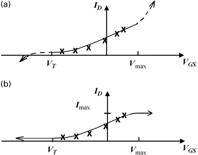
Figure 6.2 Problems caused by naïve parameter extraction methods for poorly defined constitutive relations. Data (x), models (lines). Top: Evaluation of polynomial beyond domain of validity (dashed lines). Bottom: proper extension of constitutive relations.
6.2.5.2 Properties of Well-Defined Constitutive Relations
The root cause of these problems is the formulation of the model constitutive relations themselves. Care must be used to define the domain of voltages where Eq. (6.6) applies and then to appropriately extend this domain to define the constitutive relationship properly for all values of V1V1, while imposing reasonable conditions on the global I–V relationship. We encountered a similar issue with the Shockley physical model in Section 6.2.1. Model constitutive relations must have certain mathematical properties for a robust device model. They must be well-defined for all voltages, even at values far outside the range over which a real device might operate in any application. They must be continuous functions of their arguments. Moreover, the first order partial derivatives of the constitutive relations must be continuous everywhere. Usually the second partial derivatives should be bounded as well. These conditions are imposed mainly by the underlying Newton-type algorithms used by the simulator to converge to a solution of the circuit equations, something discussed in Chapter 2.
Even for solutions known to be within a subdomain of intrinsic terminal voltages where the constitutive relations are well-behaved, the process of iterating to convergence may require the evaluation of the constitutive relations at values of the controlling variables far outside this region. If, in these extreme regions, a singularity in the function evaluation of the constitutive relation is encountered, or if the corresponding derivative values point in the wrong direction, the simulator can be led astray for the next iteration, and convergence may fail altogether. It may also happen that the simulation converges to a nonphysical solution that happens to satisfy the circuit equations.
Further constraints on constitutive relations are induced by accuracy requirements for certain types of simulations. Accuracy requirements for distortion simulation, such as IM3 or IM5 at low signal amplitudes, impose higher order continuity constraints on the model constitutive relations. That is, constitutive relations should have nonvanishing partial derivatives of sufficiently high orders. Note that the constitutive relations defined by (6.6) do not satisfy this requirement since all fourth order and higher partial derivatives are identically zero.
6.2.5.3 Regularizing Poorly Defined Constitutive Relations: An Example
The solution to making (6.6) well-defined can be obtained by enforcing additional constraints on the model – namely that it pinches off and attains a maximum value – to make it physically reasonable for all values of the independent variables. Specifically, the model channel current should be constrained to be zero for all values of voltages at or below a value of V1 = VTV1=VT, the threshold voltage. Continuity of the channel current and its first derivative at VTVT means IDSV1=VTV2=∂IDSV1=VTV2∂V1=0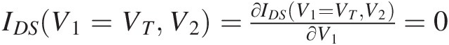 . Therefore, the cubic polynomial factor in (6.6) has a double root at V1 = VTV1=VT, allowing us to factor out (V1 − VT)2V1−VT2 from the general cubic expression, making it easier to obtain the remaining polynomial coefficients. We can also assert that there is a value, V1 = VmaxV1=Vmax, where the current attains its maximum value and is constant for all higher values of V1V1. These conditions enable us to reformulate (6.6) in terms of the three new parameters VT, Vmax, ImaxVT,Vmax,Imax as given in (6.10).
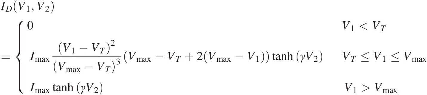 (6.10)
Equation (6.10) satisfies all the constraints required for a well-defined and reasonable constitutive relation [18–21],3 provided only VT < VmaxVT<Vmax and Imax and γImaxandγ are positive. Moreover, the new parameters now have a clear interpretation in terms of minimum and maximum values of the model current (see Exercise 6.1). However, this formulation of the model with corresponding parameter extraction methodology has used up all of the original fitting degrees of freedom in Eqn. (6.6). Distortion figures of merit, such as IM3, are completely determined by the three parameters, VT, Vmax, ImaxVT,Vmax,Imax. For real transistors, variations in the doping density can result in devices with identical values of VT, Vmax, ImaxVT,Vmax,Imax but with different shapes of the I–V curves between zero and ImaxImax. Therefore, more general and flexible constitutive relations than those of (6.10) are required to independently and accurately model intermodulation distortion. See also [22].
It should be clear from the above discussion of the channel current constitutive relation that the charge constitutive relation (6.7) also needs to be extended for values of VGSVGS approaching ϕϕ and beyond. This is easily accomplished by linearizing (6.7) at some fixed voltage, V0 < ϕV0<ϕ. The result is given by Eq. (6.11).
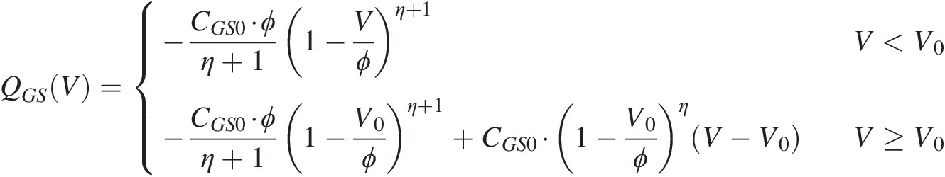 (6.11)
6.2.5.4 Comment on Polynomials for Model Constitutive Relations
Polynomials are fast to evaluate – so models using polynomial constitutive relations tend to simulate quickly. Polynomials are linear in the coefficients so their numerical values can be extracted from data efficiently and without the need for nonlinear optimization (e.g. by using least squares or pseudo-inverse methods). However, polynomials diverge for very large magnitudes of their arguments. They have only finite orders of nonvanishing derivatives, so they can cause discontinuities of simulated distortion at low signal levels. Extending the domain of polynomial constitutive relations beyond the boundary over which they are used for extraction becomes much more difficult when the expressions depend on more than one variable (e.g. both V1V1 and V2V2), unlike the simple case discussed above where the polynomial part of (6.6) depends only on V1V1. In general, therefore, polynomial constitutive relationships should be used with great care or avoided altogether if possible.
6.2.5.5 Comments on Optimization-Based Parameter Extraction
For constitutive relations more complicated than (6.10), parameter extraction generally involves a simulation-optimization loop. An example of the general flow is given in Figure 6.3. However, such direct approaches can be slow. The model must be evaluated and parameters updated many times before a good result is obtained. Gradient-based optimization schemes may be sensitive to the initial parameter values or get stuck in local minima in the cost function (the error function between the desired value and actual value of the simulation at particular values of the model parameters). There are other techniques, such as simulated annealing [23] and genetic algorithms [24] that can help find a global solution to the nonlinear optimization problem, but these techniques are usually much slower and more complex.

Figure 6.3 Optimization-based parameter extraction flow.
The parameters in (6.11) must be constrained not to take specific values during optimization where the constitutive relations might become singular (e.g., for η = − 1η=−1). Modern parameter extraction software usually allows the user to restrict the parameter values to specific ranges during the iterative optimization process.
Advanced nonlinear models (see, e.g., [25]) have complicated nonlinear electrical constitutive relations. Most of these electrical nonlinear constitutive relations have nonlinear thermal dependences as well. It is usually best to extract parameters of such models by using an iterative scheme where dominant electrical parameters are extracted from specific subsets of data to which those parameters exhibit high sensitivities. A good flow is necessary for good, global fits to the data and also to get physically reasonable parameter values, which can then be scaled to model devices of other sizes without the need for an additional comprehensive extraction.
Of course, a given model with fixed, a priori closed form constitutive relations may never give sufficiently accurate results, for any possible set of parameter values. The model may be flawed, or just too simple to represent the actual behavior of the device. We turn now to other approaches that are more flexible.
6.2.6 Table-Based Models
Table models are usually classified as extreme forms of empirical models since the constitutive relations are not physically based but depend directly on measured data. In fact, there are no fixed, a priori model constitutive relations with parameters to be extracted at all. Table models are examples of “nonparametric” models. The data are the constitutive relations. The idea is simple enough, at least for the I–V constitutive relations of a quasi-static model. For the resistive model, just measure the DC I–V curves, tabulate the results, and interpolate as needed during simulation to evaluate the constitutive relations and their derivatives during the solution of the circuit equations. For the nonlinear reactive model, much more analysis needs to be done. We will address this in Section 6.2.9.
6.2.6.1 Nonlinear Rereferencing: Extrinsic-Intrinsic Mapping between Device Planes4
The intrinsic model nonlinear constitutive relations are defined on the set of intrinsic voltages, VGSint and VDSint
 , after accounting for the voltage drop across the parasitic resistances when voltages VGSext
 and VDSext
 are applied at the extrinsic device terminals (see Figure 6.4). Measured I–V data, on the other hand, are defined on the extrinsic voltages that correspond to the independent variables of the characterization. The relationship between extrinsic and intrinsic DC voltages is simple, given the resistive parasitic element values, previously extracted, as explained in Chapter 5, and the simple equivalent circuit topology. The equations are given in (6.12) [26]. An important issue for table models, however, is that the extrinsic voltages at which the measurements are taken are usually defined on a grid, but the resulting intrinsic voltages, explicitly computed by substitution using (6.12), do not fall on a grid, and therefore cannot often be directly tabulated. This is shown in Figure 6.5.
 (6.12)
If the measured extrinsic I–V data is fit or interpolated, equation (6.12) can be interpreted as a set of implicit nonlinear equations for the extrinsic voltages, VGSextandVDSext , given specified intrinsic voltages VGSintandVDSint
 , [18,26]. Solving (6.12) in this sense enables the data to be re-gridded on the intrinsic space so that the terminal currents can be tabulated as functions of the intrinsic voltages.

Figure 6.4 Extrinsic and Intrinsic device planes for nonlinear constitutive relations re-referencing

Figure 6.5 Extrinsic (gridded) and corresponding intrinsic (nongridded) voltage domain of a FET.
Modeling the measured I–V data as functions of the intrinsic voltages reveals characteristics quite different from the model expressed in terms of extrinsic data. This is shown in Figure 6.6. In part (a) of the figure, the modeled I–V curves as functions of the applied (extrinsic) voltages VGSext and VDSext
 are plotted. In part (b), intrinsic I–V modeled constitutive relations, defined on VGSint
 and VDSint
 are plotted. There is a big difference between Figure 6a and b, especially around the knee of the curves. This process also makes clear that errors in parasitic extraction – where the values of the terminal resistances are determined – can distort the characteristics that we would otherwise attribute to the intrinsic model.

Figure 6.6 FET model I–V constitutive relations expressed as functions of (a) extrinsic and (b) intrinsic voltages.
Alternatively, one can tabulate the extrinsic I–V data, as measured on the original grid, and treat the coupled equations (6.12) as additional model equations to be solved dynamically during simulation. This allows the simulator to sense the intrinsic voltages and look up the associated interpolated values of the measured I–V curves consistent with the solution of (6.12). This saves the post-processing step of regridding during the parameter extraction but adds the two nonlinear equations (6.12) to the model, thus increasing simulation time.
Table-based models can be both accurate and general. The same procedure and modeling infrastructure can be used to model devices in very different material systems (e.g. Si and GaAs) and manufacturing processes [26]. An example of the same table-based model applied to Si and GaAs transistors is given in Figure 6.7. For physically based models, each transistor would have very different constitutive relations requiring different parameter extraction procedures.

6.2.6.2 Issues with Table-Based Models
A critical issue with table-based models is the nature of the interpolation algorithms that define the constitutive relations as differentiable functions on the continuous domain containing all the discrete data points stored in the tables. The interpolator needs to define the partial derivatives continuously, and extrapolate appropriately – the same conditions that apply to all constitutive relations. At relatively small signal levels, it has been shown that simulations of harmonic distortion can become inaccurate when the amplitude (in volts) of the signal is comparable to or smaller than the distance between voltage data-points at which the constitutive relations are sampled [27]. This is demonstrated in Figure 6.8. At small voltage swings associated with low power signals, simulation results depend on the mathematical properties of the interpolant between data points rather than the underlying data itself. For larger signals, the corresponding applied voltage swings average out the local characteristics of the interpolant, and the table-based model simulations become quite accurate. It can sometimes help to increase the density of the data points. For some spline schemes, however, this can make the interpolant oscillate nonphysically between data points. Ultimately, there is a practical limit on taking too many data points leading to increased measurement time, file size, and interpolation of noise [27].

Various types of spline-based models have been explored in the literature. Methods involving B-splines have been applied in [28], but unphysical behavior due to spline oscillations between knots can still sometimes occur. Variation-diminishing splines [29] can tame oscillations, but their low polynomial order precludes their use for intermodulation simulation. “Smoothing splines” [30] can have a variable spline order and trade off accuracy for smoothing noise.
For good large-signal simulation results with table-based models, it is necessary to acquire data over the widest possible range of device operating conditions. This range should include regions up to or just into breakdown, high power dissipation, and forward gate conduction, since these phenomena are critical to limiting the large-signal RF device performance. A portion of the domain of static measurements is shown in Figure 6.9 for a GaAs FET. The boundary illustrates the major mechanisms that constrain the data to the interior of the boundary. The precise shape depends on the detailed device-specific characteristics and the compliance limits on currents, set by the user, on the measurement equipment [31,32]. Covering a wide range of device operation during characterization reduces the likelihood of uncontrolled extrapolation during simulation and possible poor convergence as a consequence. Unfortunately, these extreme operating conditions can stress the device to the point of changing its characteristic during characterization [27]. This is especially true for static operating conditions at which DC I–V and S-parameters are measured. An excellent model of a degraded device can be obtained unless care is used. A delicate balance must be maintained between complete characterization and device safety. It is therefore very important to defer stressful static measurements until as late as possible in the characterization process [27].

Figure 6.9 Data domain for pHEMT device with compliance boundaries.
6.2.7 Models Based on Artificial Neural Networks (ANNs)
Many of the problems of table models, including issues of gridding, ragged boundaries, and poor interpolation properties, can be obviated by replacing the tables with artificial neural networks (ANNs) [33–36]. An ANN is a parallel processor made up of simple, interconnected processing units, called neurons, with weighted connections and biases that constitute the parameters [37,38]. A schematic of an ANN is given in Figure 6.10. Each neuron represents a simple univariate nonlinear “sigmoid” function, with range zero to unity, monotonically increasing, and infinitely differentiable with respect to its argument. The layer structure and interconnectedness of the neurons – specified by the weights – endows the overall network with powerful mathematical properties. The Universal Approximation Theorem states that any nonlinear function, in an arbitrary number of variables, can be approximated arbitrarily well by such a network [37].

Figure 6.10 ANN illustrating sigmoid function, layer structure, and mathematical formula.
ANNs provide a powerful and flexible way to approximate the required model multivariate constitutive relations by smooth nonlinear functions from discretely sampled scattered data. ANNs provide an alternative to using multivariate polynomials, rational functions, or other more conventional basis sets to approximate the data. There are now powerful third party software tools [38,39] available to train the networks, that is, extract the weights and biases that form the parameters of the resulting function, such that the network approximates the measured nonlinear constitutive relationship well.
A key benefit of ANNs is the infinite differentiability of the resulting constitutive relations, providing a smooth approximation also for all the partial derivatives necessary for good low-level distortion simulation.5 Another key benefit is that ANNs can be trained on scattered data. In particular, they can be trained directly on the scattered intrinsic I − VintI−Vint data without the need for regridding. An example of an ANN I–V constitutive relation trained on the nongridded intrinsic voltage space of a pHEMT device is presented in Figure 6.11. Hard constraints on model constitutive relations, such as required by discrete symmetry properties, can also be accommodated by ANN technology. Symmetry conditions are discussed in Section 6.5. An example of an ANN-based FET model with drain-source exchange symmetry is presented in [34].

Figure 6.11 (a) ANN FET I–V model (x) and data (circles). (b) Nongridded intrinsic voltage domain.
The mathematical form of an ANN nonlinear constitutive relation is a very complicated expression, typically involving many transcendental functions – even nested transcendental functions if there are multiple hidden layers. The expression can take many lines of mathematical symbols just to write out explicitly. However, from the point of view of the simulator, it is just a closed-form nonlinear expression like that of (6.10). The implementation of an ANN-based model in the simulator requires the values of the neural-based constitutive relations and their partial derivatives at all values of the independent variables, just like any conventional compact model. The parameters (weights and biases) can be placed in a datafile and read by the simulator for each model instance. The partial derivatives can be efficiently computed by evaluating a related neural network, called the adjoint network, obtained from the original network and weights [40].
6.2.8 Extrapolation of Measurement-Based Models
Conventional parametric empirical models, when properly formulated, are well-defined everywhere, even far outside the training data used to extract the parameters. As we have discussed, this can be achieved by defining the constitutive relations first in a bounded domain and then appropriately extending this domain, often by linearization.
More of a challenge is how to systematically extend the domain of table-based or ANN models. Table models based on polynomial splines can extrapolate very poorly, causing failures in convergence of simulation. An example of a table-model extrapolation is shown in Figure 6.12a. The symbols indicate the actual data points. The solid lines correspond to the table-based model. Within the region of actual data, the model fits extremely well. At high drain voltages, the model extrapolates and the model curves cross in a nonphysical way. Eventually, the drain current of the model becomes negative (nonphysical) and the model does not converge robustly.

Figure 6.12 Extrapolation of measurement-based FET models. Data (+), model (lines): (a) without guided extrapolation, (b) with guided extrapolation.
ANN models don’t diverge as rapidly as polynomials, but their extrapolation properties are also poor from the perspective of simulation robustness. Successful deployment of table-based or ANN models can depend on a good “guided extrapolation” to help the simulator find its way back into or near the training region should it stray far from the region at any particular iteration. The method reported in [41] defines a compact domain containing the training region in terms of the convex hull constructed from the data points themselves [42]. Inside this region, the table or ANN is evaluated. Outside the boundary, an algorithm is applied to smoothly extend the current constitutive relation in a way that sharply increases the model branch conductances outside the training range. An example is shown in Figure 6.12b. This method increases the robustness of DC convergence and also the maximum power levels at which the model converges in large-signal harmonic balance analysis. Transient analysis becomes more robust as well. Other methods of extrapolation of ANN models can be found in [35,43].
6.2.9 Large-Signal Model Connection to Small-Signal Data
This section shows how to establish a connection between a large-signal model and small-signal measurements, in particular, linear S-parameter measurements. This is important for a variety of reasons, but primarily for parameter extraction based on readily available, calibrated data obtained from vector network analyzer instruments.
6.2.9.1 Linearization of Large-Signal Models around a DC Operating Point
We already encountered this procedure in Chapter 3 where we derived an S-parameter model from a simple nonlinear model of a FET. Here we derive small-signal models from large-signal models more generally, but still assuming a simple lumped description. We assume the following model for the intrinsic nonlinear two-port given in (6.13). Here the index, i, goes from 1 to 2, labeling the port currents and port voltages. Equation (6.13) allows gate leakage terms in parallel to the junction capacitances at the gate, terms that can become important as the controlling voltage values approach breakdown and forward conduction during the RF time-dependent large-signal excitation.6
 (6.13)
We now assume the time-varying port voltages have a DC component, ViDC , and a small RF sinusoidal component, Virf
 , a complex phasor at the angular frequency ωω. We write the excitations as (6.14), substitute them into (6.13), compute the port current response to first order in the RF amplitudes, and finally evaluate the result in the frequency domain.
 (6.14)
The result is (6.15), describing the port current complex phasors, IiIi, associated with frequency ωω, as a linear combination of the port voltage phasors, Vjrf , at the same frequency. The small-signal model admittance matrix, Yi, jYi,j, is simply expressed in terms of the partial derivatives of the port current and charge constitutive relations from the linearization of (6.13), according to (6.16). Here we introduce the real conductance and capacitance matrices, GG and CC, respectively, into which the complex admittance naturally separates.
 (6.15)
 (6.16)
If we identify ports 1 and 2 with the gate and drain (common source configuration with the specified ordering), then we can write the matrix (6.16) in terms of elements indexed with the letters corresponding to gate and drain, as in (6.17).
 (6.17)
From the analysis of Chapter 5, we had an independently derived expression for the measured intrinsic admittance matrix, expressed in terms of the ECPs based on the specific linear model topology considered. We reproduce equation 5.18, here for convenience as (6.18).
 (6.18)
Equating (6.17) and (6.18), matrix element by matrix element, we can identify simple linear combinations of the measured linear ECPs at any particular bias point with specific partial derivatives of the large-signal model constitutive relations evaluated at the corresponding bias. Even more generally, without any reference to the linear model equivalent circuit topology, the correspondence of (6.17) and (6.18), predicts that the intrinsic admittance matrix element values, obtained from the measured S-parameter data, should equal the partial derivatives of the large-signal model constitutive relations at the corresponding DC bias condition. This conclusion follows quite generally from the quasi-static large-signal modeling assumption that the intrinsic device can be modeled as a parallel combination of lumped nonlinear current sources and nonlinear charge sources. This assumption will be tested and analyzed extensively throughout the rest of this section.
6.3 Charge Modeling
6.3.1 Introduction to Charge Modeling
Nonlinear charge modeling has been shown to be critical for accurate simulation of bias-dependent high-frequency S-parameters [44], intermodulation distortion and ACPR in FETs [45,46], and harmonic and intermodulation distortion in III-V HBTs [47–50]. FET models with identical equivalent circuit topologies and identical I–V constitutive relations, differing from one another only by the form of their Q–V constitutive relations, can result in differences of 5–10 dB or more in simulated IM3 and differences of more than 5 dB in simulations of ACPR [45]. Moreover, conventional nonlinear charge models, based on textbook junction formulae, tend to show significant discrepancy compared to actual measured device characteristics.
The charge modeling problem can be simply stated as the specification of the nonlinear constitutive relations defining the independent charges at the (intrinsic) terminals of the circuit model, as functions of the relevant independent controlling variables, usually voltages. The charge-based contribution to the current at the ith terminal is then the total time derivative of the charge function, Qi. This is expressed in (6.19). If we choose one of the three terminals as a reference to define a particular 2-port description, we can interpret Qi as the charge function at the ith independent port.
 (6.19)
Here V1V1 and V2V2 are the two independent intrinsic port voltages, which, for a FET, can be taken to be VGSVGS and VDSVDS. For an HBT, V1V1 and V2V2 can be taken to be VBEVBE and VCEVCE. I1I1 is the gate (base) current and I2I2 is the drain (collector) current for the FET (HBT) cases, respectively. Charge constitutive relations contribute to the current model through the time derivative operator in (6.19). This makes it apparent that charge plays an increasingly important role as the stimulus frequency increases.
The Curtice charge model with branch elements given by (6.7) and (6.9) can be cast in terms of terminal charges at the gate and drain, respectively, according to (6.20). Included in (6.20) is an additional nonlinear charge-based capacitor to model the drain-source capacitive coupling [11]. We see that the total terminal, or port charge function, is just the sum of the charges associated with all branch charges attached to the terminal with an appropriate reference direction. The arguments of (6.20) are time-varying intrinsic voltage differences.
 (6.20)
For a three-terminal intrinsic model with gate and drain charges, Kirchhoff’s Current Law (KCL), constrains the model to also have a charge function associated with the source node equal and opposite of the sum of the drain and gate charges. That is, we must have (6.21). Strictly speaking, the right-hand-side of (6.21) can be any constant, but we can set the constant to zero since the charges only enter the circuit equations in terms of a total time derivative. In the port description, we only need to define two independent port charge functions, Q1 and Q2.
 (6.21)
We note that (6.21) is a circuit-level expression of physical charge conservation, a consequence of KCL and is to be carefully distinguished from the independent modeling concept that we will refer to by terminal charge conservation, to be introduced in Section 6.3.4.
The Shockley charge model (6.4) and the Curtice charge models (6.7) and (6.8), evidently fit into the form (6.20). In both the Curtice and Shockley models, the gate charge expressions separate into the sum of two functions, each defined on one variable only. For the Curtice model, this is also the case for the drain charge as evident from (6.20). It is a consequence of the idealized simplicity of these models that there are only two one-dimensional functions, QGS(V)QGSV and QGD(V)QGDV, defining the entire two-port Shockley charge model, and three one-dimensional functions, QGS(V)QGSV, QGD(V)QGDV, and QDS(V)QDSV, defining the entire two-port Curtice charge model. The more general equation (6.19) is defined in terms of two arbitrary functions of two variables, QG(V1, V2)QGV1V2 and QD(V1, V2)QDV1V2, neither of which needs to be separable in terms of sums of univariate functions.
6.3.2 Measurement-Based Approach to Charge Modeling
Unlike DC I–V curves, charge constitutive relations cannot be measured directly. To specify the charge model, it is most convenient to establish a relationship between the model nonlinear charge constitutive relations and simpler quantities that can be directly obtained from bias-dependent S-parameter data. In fact, these relationships have been established by equating the imaginary parts of (6.17) and (6.18).
Assuming a particular two-port configuration, we obtain the following matrix equation, which relates the four nonlinear functions of bias constituting the imaginary parts of the admittance matrix, to the partial derivatives of the two model nonlinear charge functions, QiQi, evaluated at the operating point. Here indices i and j range from 1 to 2, the number of ports. For devices like MOSFETs, with additional terminals (e.g. bulk), i and j range from 1 to 3. The right-hand equality defines a capacitance matrix, CijCij, used for notational simplicity.
 (6.22)
The assumption that the middle and right-hand side of (6.22) are independent of frequency is necessary for consistency with (6.19). In Chapter 5 we showed examples of measured device data consistent with the left-hand side of (6.22) being independent of frequency. In practice, with a good intrinsic and extrinsic equivalent circuit topology, and good parasitic extraction, (6.22) is approximately true for frequencies approaching the cutoff frequency of the device. For higher frequencies, the intrinsic model topology needs to be augmented, such as adding additional elements in series with the nonlinear capacitors, to deal with “non quasi-static effects.” We described such RGS and RGD elements, for example, in Chapter 5, Section 5.6.5.2 for the small-signal model. For the large-signal model, however, this is a more difficult problem, and we won’t deal with it further here.
The measured admittance parameters can be obtained by simple linear transformations of the (properly de-embedded) S-parameters according to (6.23), which is equivalent to 3.36 (see also [51]). The measured common source capacitance matrix then follows by taking the imaginary part of (6.23) and dividing by angular frequency.
 (6.23)
At this point, modeled and measured intrinsic imaginary admittance functions, or equivalently, the capacitance matrix elements, CijCij, can be directly compared.
However, it is more customary to compare modeled and measured small-signal responses in terms of linear equivalent circuit elements. There are many different intrinsic linear equivalent circuit representations that lead to the same intrinsic capacitance matrix. An alternative will be presented in Section 6.3.3. Defining equivalent circuit elements therefore requires a specific choice of equivalent circuit topology.
The linear equivalent circuit shown in Figure 5.27 maps, via the imaginary part of 5.18, the elements into the four independently measured capacitance matrix elements defined by 5.18. We solve these equations for the ECP values in (6.24). When applied to the transformed S-parameter measurements using (6.23), equations (6.24) define “measured” equivalent circuit elements. When applied to the linearized model admittances, (6.24) results in “modeled” equivalent circuit elements.
 (6.24)
We note that there are four capacitance-equivalent circuit elements defined by Eq. (6.24). This is not surprising given that there are four functions, CijCij, corresponding to the four imaginary parts of the two-port admittance matrix. However, there are only three nodes in the equivalent circuit diagram of Figure 6.13. Historically, it was customary to place one capacitance between each pair of nodes. This procedure neglected, entirely, the fourth element, CmCm, called the transcapacitance. As shown in Chapter 5, its contribution to the small-signal data is very significant.

Figure 6.13 Linear equivalent circuit model of capacitance part of intrinsic FET model. See also Figure 5.27.
A three-terminal (two-port) intrinsic equivalent circuit with two independent terminal charges generally leads to (at least) one transcapacitance. The equivalent circuit of Figure 6.13 or equivalently (6.24), places the transcapacitance in the device channel branch connecting drain and source, (parallel to the transconductance as is shown in Figure 5.27). It is important to note that the relationship of terminal charge partial derivatives to admittance matrices given in (6.22) is unique and is more fundamental than the set of transformations that define linear equivalent circuit elements in Eq. (6.24).
6.3.3 Nonuniqueness of Equivalent Circuits
Here we demonstrate another way of looking at transcapacitances, starting from an equivalent circuit that looks a little different from that of Figure 6.13.
We consider the topology given by Figure 6.14. Another possibility is given in [52].

Figure 6.14 Alternative linear equivalent circuit for capacitance model of a FET.
The elements in this circuit are defined by how they produce port currents, which is given by (6.25). Note that there are two capacitances and two transcapacitances in this description corresponding to the equivalent circuit of Figure 6.14, whereas the equivalent circuit of Figure 6.13 had three capacitances and one transcapacitance.7
 (6.25)
The common gate capacitance matrix corresponding to (6.25) is given in (6.26).
 (6.26)
The forms of (6.25) and (6.26) are very simple and symmetric, and lend themselves to easier expressions for drain-source exchange symmetry. There is also a unique identification of the ECPs of Figure 6.14 and the common-gate imaginary part of the admittance parameters. This is even simpler than the linear combinations of common source Y-parameters needed to identify the ECPs of Figure 6.13 using (6.24).
Again we note that at a general bias condition, XSG≠XDGXSG≠XDG and so (6.26) is still not reciprocal, just like (6.24). If the device model has a nonreciprocal capacitance matrix in any port configuration, the conclusion is that the two-port model admits a transcapacitance.
From the point of view of the terminal charges, the results work out exactly the same, independent of where the transcapactiance element is placed in the equivalent circuit. The gate, drain, and source charges will have precisely the same functional forms on a fixed set of port voltages whether recovered from common gate Y-parameters using the topology of Figure 6.14 or common source Y-parameters using the topology of Figure 6.13.
Using (6.24), the measured capacitances can be compared to theory. An example of measured capacitances, as functions of the bias conditions, is given by Figure 6.15 for a GaAs pHEMT. Several facts are immediately apparent from the figures. The value of the transcapacitance, CmCm, is generally zero or negative. This follows from the discussion in Chapter 5 related to equation (5.21). CGSCGS depends not just on VGSVGS, the voltage across the element, but also on the other independent voltage, VDSVDS. This is qualitatively different from the Shockley and Curtice models, where the model CGSCGS is completely independent of VDSVDS. This also means that CGSCGS cannot be modeled by a standard two-terminal nonlinear capacitor,8 for any functional dependence on the (single) voltage, VGSVGS, across the element. The feedback capacitance, CGDCGD, depends on both VGSVGS and VDSVDS, in a more complicated way than VGD = VGS − VDSVGD=VGS−VDS. That is, CGDCGD also cannot be modeled by a standard two-terminal nonlinear capacitor, despite the familiar looking symbol in the linear equivalent circuit. Moreover, the VGSVGS dependence of CGDCGD, for large VDSVDS, when the device is in the saturation region of operation, is exactly the opposite of the Shockley model’s prediction. That is, the feedback capacitance is actually much larger when the device is pinched off (VGS = − 2VVGS=−2V) than when the channel is open (VGS = − 1.2VVGS=−1.2V) and conducting current. More elaborate physical theories, which yield results closer to measured characteristics of modern FETs, lead to equations sufficiently complicated that they can be expressed, usually, only in approximate form [53]. A more recent approach, based on a decomposition of the charge model into simple one-dimensional depletion charges and a two-dimensional drift charge defined in terms of voltage and current, has been proposed in [54] and is presented in Section 6.3.9.

Figure 6.15 Bias-dependence of GaAs pHEMT capacitance matrix elements. VGS ranges from −2 V to −1.2 V in 0.2 V steps. The arrows point in the direction of increasing VGS.
6.3.4 Terminal Charge Conservation
The above development, beginning with (6.19), started from large-signal model equations and then computed the small-signal responses that can be compared easily to measured S-parameter (Y-parameter) data. In what follows, we present a treatment based on trying to reverse the above flow. That is, we seek to solve the inverse problem to determine the functional form of the large-signal model constitutive relations, QiQi, that enter (6.19), directly from the measured bias-dependence of the small-signal characteristics. Unfortunately, but not surprisingly, this inverse process is generally ill-posed. However, under certain specific and verifiable conditions, a practical inverse modeling process can be constructed for transistors manufactured in a variety of material systems. This enables the generation of accurate nonlinear circuit simulation models for devices of great practical utility, from simple DC and linear (S-parameter) measurements.
Equation (6.22), with the left-hand side referring to measured data, can be interpreted as the mathematical statement of the inverse problem. That is, the measured bias-dependences of the intrinsic admittance elements are equated to the partial derivatives of the respective model terminal charges. The mathematical problem then becomes determining the conditions under which (6.22) can be solved for the model terminal charge functions, QiQi.
The necessary and sufficient conditions for the terminal charges to be recovered from bias-dependent capacitance matrix elements defined from measured data using Equations (6.22), are succinctly expressed by (6.27) [26,31,55].
 (6.27)
Through definitions (6.22), equations (6.27) are constraints on pairs of bias-dependent measured admittances, one pair per row of the admittance matrix labeled by the index i. If (6.27) is satisfied, then the terminal charges can be constructed directly from the measured capacitance matrix elements by a path-independent contour (line) integration expressed by (6.28).
This result is unique up to an arbitrary constant that has no observable consequences and so the constant can be set equal to zero. Moreover, the partial derivatives of this charge reduce exactly to the measured bias-dependent capacitance measurements. That is,
 (6.29)
If (6.27) is not exactly satisfied for fixed index, i, then, strictly speaking, there is no function, Qimodel , that is consistent with (6.29). In this case, the line integral using measured capacitance functions in Eq. (6.28) produces charge functions that depend on the path chosen for the contour. Different contours produce models that fit some capacitances versus bias better than others, with no perfect fits of all capacitances possible.
Equations (6.27), expressing the equality of mixed partial derivatives with respect to voltages of different capacitance functions with the same first index, can be interpreted as meaning that pairs of capacitance functions attached to the ith node form a conservative vector field in voltage space [31]. An alternate but mathematically equivalent representation of this concept is presented in [56]. Capacitance functions that obey (6.27) are said to obey “terminal charge conservation at the ith node.”9 We use the nomenclature terminal charge conservation to distinguish it from the fundamental physical law of charge conservation that is embodied in circuit theory by Kirchoff’s Current Law (KCL) [compare (6.21) that embodies KCL]. In contrast, terminal charge conservation is a constraint that can, but needs not, be imposed by the modeler to approximate the behavior of a device. Physical charge conservation is a fundamental physical law and a requirement of any circuit model that is consistent with KCL. An example of a nonlinear model not consistent with terminal charge conservation, and its consequences, is presented in Section 6.3.7.
Any model starting from Eq. (6.19) has model capacitance functions that conserve terminal charge at each node. This is true because the model capacitances are derived in (6.22) starting from model charges and then (6.27) follows from the derivative properties of smooth functions. However, starting from independent measurements and trying to go back to model charges via (6.29) requires the constraints (6.27) to be satisfied by the measured Cijmeas data.
data.
The degree to which actual bias-dependent admittance data is consistent with the modeling principle of terminal charge conservation was investigated in [44] and [57]. For small GaAs FETs, it was found to hold extremely well at the gate, and slightly less well at the drain. For larger, high-power GaN HEMTs, these relationships don’t seem to hold quite as well, and more elaborate models are required (see Section 6.6). The applicability of terminal charge conservation to III-V HBTs was discussed in [58] and [60] and found to be extremely useful in accurate modeling of delays and “capacitance cancellation” effects in such transistors.
6.3.5 Practical Considerations for Nonlinear Charge Modeling
The parameterization of line-integral (6.28) for two distinct paths, shown in Figure 6.16, are written explicitly in (6.30) and (6.31), respectively. Path independence means the same charge function can be computed from completely independent sets of bias-dependent data along the two paths of Figure 6.16.
 (6.30)
 (6.31)
Figure 6.16 Two different paths in voltage space for line-integral calculation of terminal charges.
There are several issues with respect to implementing (6.30) and (6.31) directly on measured data. The measured capacitance data is defined only at the discrete voltages (points of in Figure 6.16) so the integrals have to be done numerically. If the data is not on a rectangular grid, interpolation along some of the paths may be required (as in in Figure 6.16 along the VGSVGS direction). Fundamentally, if (6.27) is not exactly satisfied due to measurement errors or the neglect of effects like temperature and traps (to be considered later), the different paths effectively trade-off model fidelity of ImY12ImY12 and ImY11ImY11 versus bias, respectively. Integration error accumulates for large paths so the charge value at points far away from the starting point of integration (VG0VG0 and VD0VD0) will be less accurate. The integration is also difficult to perform along paths to or near the ragged boundary of the data domain (see Figure 6.16).
Despite these practical difficulties, table-based models using full two-dimensional nonlinear gate charge functions constructed directly from small-signal device data have found their way into practical commercial tools [59]. Table-based charge models can be much more accurate than closed form empirical models, where the complex two-dimensional nature of the Q-V constitutive relations have not received as much attention as have I–V relations which are directly measureable.
6.3.6 Charge Functions from Adjoint ANN Training.
There are now robust methodologies to train ANNs to construct Q-V constitutive relations directly from knowledge of the desired function’s partial derivatives as represented by measured capacitances [33,40]. This has been a major breakthrough for practical measurement-based charge modeling of transistors.
All the practical problems described above of computing multidimensional charge functions by line integration of suitably decomposed small-signal data are ameliorated by using the adjoint ANN training approach [40]. This method directly results in a neural network that represents the Qi(VGS, VDS)QiVGSVDSfunctions from information only about their partial derivatives, as represented by the bias-dependent measured capacitances defined by (6.29). A diagram of the training method is given in Figure 6.17. If (6.27) is not exactly satisfied by the device data, the adjoint method still returns a charge function that generally gives a much better global compromise between the capacitances than the typical line-integral methods. The training can take place directly on the intrinsic nongridded intrinsic bias data, and the ragged boundary presents no difficulty. Validation of the adjoint ANN approach to simultaneously fit the detailed two-dimensional FET input capacitance behavior with bias is shown in Figure 6.18. The validation for the independent fit for the drain capacitances is shown in Figure 6.19.

Figure 6.17 Adjoint ANN training of model gate terminal charge function from C11 and C12 data.


Figure 6.19 Validation of ANN-based drain charge model fitting, (a) C21, (b) C22. Data (symbols), model (lines); (c) gate charge function, QD.
With current-voltage and charge-voltage nonlinear constitutive relations modeled by ANNs, the improvement in simulation accuracy over spline-based table models can be demonstrated. A comparison is shown for the case of a GaAs pHEMT device in Figure 6.20. At moderate to high power levels, where the voltage swings are comparable or greater than the distance between discrete data points, the ANN and table-based models are nearly identical and compare well with measurements. At low power levels, the distortion simulation of the table-based model is determined by the numerical properties of the interpolating functions. Piecewise-cubic splines, used in this case, don’t do a good job for high-order distortion at low signal levels, hence the ragged variation of distortion with power. However, the ANN model is very well-behaved at all power levels, and has the correct asymptotic dependence as the power decreases.

6.3.7 Capacitance-Based Nonlinear Models and Their Consequences
Strictly speaking, if (6.29) is not exactly satisfied, the assumption that (6.19) models the non-current-source terms in the intrinsic device is not consistent with the data. An alternative is to write the time-dependent port currents directly in terms of the measured two-port capacitance matrix elements [26,60]. That is, one can propose to replace (6.19) with more general equations according to (6.32).
 (6.32)
In (6.32) the model functions Ci1Ci1 and Ci2Ci2 can be completely independent of one another, without the constraints of (6.27). It is quite easy to implement models like (6.32) for non terminal-charge-conserving capacitance-based large-signal equations in nonlinear circuit simulators. Equivalently, using the definitions (6.24), it is possible to rewrite (6.32) in terms of contributions from the four equivalent circuit elements of Figure 6.13 [26]. Compared to (6.19), which is specified by two nonlinear functions, (6.32) is defined by four model nonlinear functions (for a two-port device), which, if desired, can be taken to be precisely the measured (or independently fit) relations from equation (6.24). Such a model will exactly fit the measured bias-dependent small-signal dependence, by construction. However, as proved in [19,52,60,61] such models will generally lead to spectra containing a DC component, proportional to the stimulus frequency and the square of the signal amplitude, generated from such capacitance elements when simulated by large signals at the device terminals [18,26,55,62]. The spectra of non termincal-charge-conserving capacitance models and terminal charge conserving models are shown in Figure 6.21a and b, respectively. A spectrum with a DC component cannot result from true displacement current, the physical origin of gate current (neglecting leakage) in reverse biased FETs due to modulated stored charge. Things are less clear in the channel of a FET, where current arises by a combination of charge transport and time varying electric field [63]. Nevertheless, enforcing terminal charge conservation on large-signal intrinsic models results in a simpler model, with no “strange” consequences in large-signal analysis. Finally, it is possible to model the gate current using Equation (6.19) (for i = 1) and the drain current using (6.32) (for i = 2). That is, terminal charge conservation can be enforced at the gate terminal but not at the drain terminal, if desired.

Figure 6.21 Spectra generated by (a) non terminal-charge-conserving gate capacitances and (b) gate terminal charge based model.
6.3.8 Transcapactiances and Energy Conservation10
The transcapacitance, CmCm, clearly shows up in device small-signal data as evidenced in Figure 6.15 (see also [64]). However, attempts to calculate stored charge from simple theoretical conditions including energy conservation leads to the conclusion that Cm = 0Cm=0, which is inconsistent with the small-signal data [26,65,66]. The magnitude of the channel current can increase with signal frequency in models that have large-signal terminal charges that admit transcapacitcances (this is the general case unless the mixed partial derivatives of the terminal charge functions are equal). This can cause an anomalously large simulated gain at high frequencies. Fortunately, the model parasitic network limits the rate of intrinsic voltage variation to a maximum frequency determined by the total input resistance and input capacitance product, partially mitigating the undesirable consequences.
The modeling principle of energy conservation for charge modeling begins with the assumption that all the electrical stored energy of an active device is computable only from the terminal charges [61]. The mathematical embodiment of stored energy-based terminal charges is perfectly analogous to that of the principle of terminal charge-based capacitance functions. That is, we would like to compute the function, U, called the co-energy, such that, for arbitrary terminal charge functions, QiQi, (6.33) holds for i=1,2 in the case of the two-port considered here [66]. It is important to emphasize that the co-energy, U, is generally not the same as the stored energy, W, even though they have the same units. There is a relationship between these functions that will be presented in equation 6.39.
 (6.33)
The formal relationship between (6.22) and its consequences, and (6.33), implies that for given terminal charge functions, QiQi, there is a unique (up to a constant) solution of (6.33) for U if and only if the terminal charge functions satisfy (6.34). If (6.34) is not satisfied, there is no solution to (6.33).
 (6.34)
Assuming for the moment that (6.34) is satisfied, we can write a hierarchy of conservation principles according to Figure 6.22.

Figure 6.22 Computation of terminal charges and capacitance matrix elements from co-energy function.
Assuming (6.33) admits a solution for U, we can formally assume a general co-energy function and try to fit the resulting capacitance functions. For example, we can write
 (6.35)
Then using (6.33) we can derive the forms for Q1 and Q2. Finally, taking partial derivatives of the charges gives us expressions for the four elements of the capacitance matrix, Cij. We can try to determine the set of coefficients, Anm, to best fit the measured capacitance matrix elements. However, this methodology raises an interesting question. We will find that we get only three unique expressions for the four capacitance matrix elements. In fact, we recognize equation (6.34) is a constraint on the bias-dependence of the terminal charge functions. Is this constraint satisfied by the data? We already know the answer. In fact, assuming only that the terminal charge functions are smooth [such as example (6.35)], (6.34) immediately leads to a reciprocal capacitance matrix (6.36).
That means the transcapacitance, derived from a co-energy function, must vanish at all bias conditions [see the last of equations (6.24)]. The off-diagonal elements of the capacitance matrix are equal, since they are the mixed partial derivatives of the same co-energy function, U, assumed to be smooth. This is summarized in (6.37). Models that start only with the presumption of terminal charge conservation, but without the additional constraint of energy conservation, are less restrictive in terms of the resulting capacitance matrix elements, which can generally admit nonreciprocal capacitance matrices, as summarized in (6.38). A hierarchy of conservation laws is shown in Figure 6.22.
 (6.37)
 (6.38)
However, such a conclusion is clearly at odds with the experimental data as shown in Figure 6.15. So we are now in a quandary. The clear evidence for a nonzero bias-dependent transcapacitance element is seemingly inconsistent with a simple embodiment of conservation of stored energy. Of course the basic physical law of energy conservation can’t be violated, so we will need to expand the model to be compatible with physics on the one hand and the data on the other.
Energy conservation constrains the model terminal charge constitutive relations in precisely the same mathematical way that terminal charge conservation constrains the capacitance functions attached to a charge-based node. Since the mixed partial derivatives of U are equal, capacitance matrices are necessarily reciprocal and there is no model transcapacitance.
The energy function, W, can be derived from the co-energy function, U according to (6.39).
 (6.39)
This is consistent with the definition of stored energy in circuit theory given by (6.40) (see [66,67]).
6.3.9 FET Charge Modeling in Terms of Depletion and Drift Charges11
We saw in Section 6.3.3 that the bias-dependence of the measured FET capacitances, shown in Figure 6.15, could not be accurately modeled by simple lumped nonlinear two-terminal capacitors controlled by the single voltage difference across the respective branch elements. The multivariate approach of Sections 6.3.4 through 6.3.6, based on terminal-charge conservation principles, was able to produce models capable of accurately reproducing the complicated two-dimensional characteristics, as demonstrated in Figures 6.18 and 6.19. But this procedure does not give much insight into the origins of this bias-dependent behavior. That is, the complexity of the mathematical formalism obscures the simple physical relationship between carrier transport and charge storage mechanisms responsible for the behavior exhibited in Figure 6.15.
An approach that suggests the origins of this behavior was proposed in [54] and will be reviewed here, in a slightly simplified form. It is based on a previous application of terminal charge conservation modeling principles to large-signal HBT models [58,60,68].
We postulate here that the total FET charge model can be constructed from a simple depletion model of separable two-terminal nonlinear charge-based capacitors, with the addition of a new voltage and current-dependent “drift charge” term. The depletion capacitors have the simple one-dimensional dependence on the single voltage difference across the elements, just like the Shockley and Curtice models, expressed by (6.20). The drift charge is a two-dimensional function, depending on one voltage, which we take as VGDVGD (based on VBCVBC used in the HBT case), and the channel current, IDID. The charge model is given by (6.41). We assume for convenience the model is defined only for VDS, ID ≥ 0VDS,ID≥0; it can be globally extended using the methods of Section 6.5.
 (6.41)
The drift charge of a unipolar FET device plays the role of the diffusion charge of a bipolar HBT transistor. The idea is that the physical charge carriers responsible for the transport current, moving at the saturated velocity, modify the otherwise simple bias-dependent contribution to the imaginary part of the intrinsic model admittance from the depletion capacitances. The velocity is inversely proportional to a transit delay, ττ, that itself depends on bias and can be extracted from simple S-parameter measurements.
The interpretation of QdriftQdrift as a drift charge requires that it vanish when no current flows. This is expressed by equation (6.42), and this property will be confirmed by the final expression to be derived.
At VDS = 0VDS=0 we can assume ID = 0ID=0 and hence Qdrift = 0Qdrift=0, simplifying (6.41) for the identification of the depletion charges. We identify the simple univariate nonlinear depletion capacitances, CGS(V) and CGD(V)CGSVandCGDV from the (intrinsic) admittances, (6.43), evaluated at VDS = 0VDS=0, as functions of the reverse bias voltage, V = VGSV=VGS. The depletion charges, QGS(V) and QGD(V)QGSVandQGDV, follow from (6.43) by simple one-dimensional integration with respect to VV. Measured and modeled gate depletion capacitances for a GaAs pHEMT are shown in Figure 6.23. The shapes are consistent with simple one-dimensional depletion physics, as expected. This means simple physically based constitutive relations can be used for this part of the nonlinear charge model, rather than just numerical calculations from measured data.
 (6.43)
We now define a transit delay function, τ(VGD, ID)τVGDID, in terms of the partial derivative of the model drift charge function with respect to the drain current. With this definition, and using (6.41), we can identify τ(VGD, ID)τVGDID from small-signal measurements by subtracting the depletion capacitance contribution from the imaginary part of the intrinsic admittance after changing variables to the pair VGD and IDVGDandID. The result is (6.44).
 (6.44)
Since we started from a charge-based model, (6.41), we know that there is a corresponding partial derivative of the drift charge with respect to the voltage, VGDVGD, which defines an effective capacitance according to (6.45)12.
 (6.45)
We know from the discussion in previous sections that terminal charge is conserved at the gate, and given the results of Exercise 6.4, we can use the adjoint training procedure of 6.3.6, in VGD, IDVGD,ID coordinates, to compute the model function, QdriftQdrift, where the right-hand sides of (6.44) and (6.45) are provided from bias-dependent RF data.
The insight comes from realizing that QdriftQdrift can be evaluated by a path-independent contour integral involving τ(VGD, ID)τVGDID and CGDdriftVGDID , as shown in (6.46). But since we must have CGDdriftVGDID=0=0
 from (6.42), we can choose a convenient contour where only one leg is nonzero, and we have the very simple result (6.47), which vanishes at ID = 0ID=0 verifying (6.42). Note that result (6.47) means that we don’t even need (6.45) to compute QdriftQdrift.
 (6.46)
 (6.47)
The bias-dependent delay, recoverable from the modeled drift charge computed from data on a GaAs pHEMT, is shown in Figure 6.24. The delay function can be directly related to the velocity-field characteristics of the III-V semiconductor transport curves, enabling modeling from a physical perspective.

Figure 6.24 Bias-dependent delay from GaAs FET drift charge model.
The charge model (6.41) fits the bias-dependent admittance data quite well [54]. It provides nearly the same accuracy as that of the general charge-based model (6.28), but with the benefit of separately identifying the depletion and transport mechanisms that, in combination, account for the overall behavior exhibited in Figures 6.15, 6.18, and 6.19. Moreover, if the drain current model includes thermal effects, then incorporating the drain current dependence in the drift charge automatically includes the temperature dependence into at least part of the reactive model, as emphasized in [69].
This approach has the potential for enabling intuitive and accurate bottoms-up analytical expressions for empirical and physically based FET models, while preserving the simple principles of device operation.
6.4 Inadequacy of Quasi-Static Large-Signal Models
This section uses the connection between partial derivatives of large-signal constitutive relations and linear data derived in 6.2.9.1 to demonstrate that the fundamental quasi-static assumption is not satisfied.
Specifically, the equality of real matrix elements on the bottom rows of (6.17) and (6.18) constitutes a prediction that the derivatives with respect to VGSVGS and VDSVDS, of the DC drain current constitutive relation should numerically equal the transconductance and output conductance, respectively, as measured at RF and microwave frequencies. That is, the DC and RF conductances should be equal.
These predictions beg to be tested experimentally. To do so we have to account for parasitic resistances consistently between DC and RF cases, to properly take the partial derivatives of the currents with respect to the intrinsic voltages, and to de-embed the S-parameter data.
6.4.1 Non-Quasi-Static Conductances
Figure 6.25 shows direct comparisons of measured data versus bias for a GaAs pHEMT transistor. There is a significant difference between the DC and RF characteristics over most of the bias range. We note that the value of the DC output conductance, GDS, can even become negative at some biases. The data in Figure 6.25 is typical of real microwave transistors and therefore proves that the quasi-static modeling assumption is not justified. This confirms the statement made in Section 6.2.3. We can express the failure of the quasi-static approach through (6.48). The simple textbook relations don’t hold! The discrepancy between device properties at DC versus RF conditions is sometimes referred to as frequency dispersion. It can have multiple causes, some of which we will examine in more detail, in particular in Section 6.6.
 (6.48)
The inadequacy of a quasi-static model is further supported by the analysis of the tradeoffs shown in Figure 6.26. The top two plots show (left to right) a quasi-static model for the channel current constitutive relation that fits the DC I–V curves very well but predicts poorly the RF conductances. The bottom two plots show (right to left) a quasi-static model for the channel current constitutive relation that fits well the bias-dependent RF data but poorly predicts the DC I–V curves. This is a fundamental limitation of the quasi-static approach, independent of the details of the constitutive relations for modeling real devices.

Figure 6.25 Measured conductances from DC data and RF data versus extrinsic bias for a GaAs pHEMT.

Figure 6.26 Inability of quasi-static models to simultaneously predict DC I–V characteristics and bias-dependent RF data.
6.4.2 High-Frequency Current Model
Just as we did to try to compute terminal charges from pairs of bias-dependent capacitance functions, we can try to find a single model function, IDRFVGSVDS , such that its distinct partial derivatives fit, simultaneously, the measured RF conductances, GmRFVGSVDSandGDSRFVGSVDS
 . The mathematical conditions for a solution of this problem are the same as discussed in Section 6.3.4, relating charge functions to pairs of capacitance functions. We know therefore, there is a unique solution provided the measured RF conductances satisfy the condition (6.49). This implies there is a relationship between the bias-dependent data, through (6.48), that can be directly tested [57].
 (6.49)
If and only if (6.49) is satisfied we can construct the model function IDRFVGSVDS uniquely up to a constant [usually fixed by requiring IDRFVGS=0VDS=0=0
 ], using the relationship (6.50). The contour integral expressed by (6.50) is path-independent if (6.49) is satisfied.
 (6.50)
 (6.51)
Both small-signal measured conductances are then perfectly recoverable from the single model function, IDRFVGSVDS according to (6.51).
Condition (6.49) is approximately satisfied for many devices over a reasonable range of bias conditions, but not perfectly. It does not hold as well for large power transistors over the full bias range. The expression (6.50) can be used to construct the model function, IDRFVGSVDS , but the result will have some residual path-dependence since (6.49) is not exactly satisfied. Alternatively, the adjoint neural network method can be used to compute an optimal solution to (6.51), that trades off errors in fitting the RF transconductance with that of the RF output conductance.
The adjoint training method was in fact used to produce the fit in the lower right plot of Figure 6.26 to GDSRF and also GmRF
 (not shown). The constructed IDRFVGSVDS
 function is depicted by the set of solid lines in the lower left plot of Figure 6.26. It is evident from this plot, as expected, that IDRFVGSVDS≠IDDCVGSVDS
 .
.
Some quasi-static models are based on substituting constitutive relation IDRFVGSVDS for the constitutive relation IDDCVGSVDS
 and ignoring the error at DC. This will certainly improve the prediction of the RF model behavior but, as we have seen, will degrade the DC fit thus causing problems with biasing of multiple transistor models with DC coupling. For some calculations, such as power added efficiency, both the RF large-signal behavior and the DC behavior must be predicted simultaneously.
Is it possible to somehow use both constitutive relations, IDRFVGSVDSandIDDCVGSVDS , in a non-quasi-static model together so as to be correct at DC and also at RF? One such phenomenological approach was taken in [31] and later [33], which combined the two constitutive relations to define an effective channel current in terms of the solution of the linear differential equation given by (6.52). Here IDRFVGStVDStandIDDCVGStVDSt
 are understood to mean the constitutive relations constructed from the bias-dependent RF and DC data, respectively, evaluated at the time-dependent intrinsic voltages during the simulation. The frequency-dependent small-signal model resulting from linearizing (6.52) smoothly transitions from the DC conductances to the RF conductances, at a characteristic frequency given by τ−1τ−1. This parameter is estimated as the time constant in a one-pole approximation to the thermal or trapping response.
 (6.52)
Analytical models, specifically the EEHEMT model [14], also use both IDRFVGStVDStandIDDCVGStVDSt constitutive relations and combine them to produce a non-quasi-static model. In this case, the two functions IDRFVGStVDStandIDDCVGStVDSt
 have the same functional form but are independently extracted to RF and DC data, respectively, so they have different numerical values for the parameters.
Such phenomenological approaches to non-quasi-static models have had considerable success over the past 25 years. However, they may result in unphysical results when used in certain large pulsed transient applications. With the power presently available in standard engineering workstations, and the evolution of fast, reliable nonlinear simulators, it is preferable to instead model the basic phenomena, namely dynamic self-heating and trapping effects, that are known to be responsible for the non-quasi-static effects in the first place. These topics will be addressed in Sections 6.6 and 6.7.2.
6.5 Symmetry
When a device or system is physically transformed in some way, but an observable property doesn’t change, we say the property is invariant with respect to that transformation. For such a case we say the device or system has a particular symmetry. A simple example is afforded by a circle. If a circle is rotated by an arbitrary angle around its center its shape is invariant. It has a (continuous) symmetry of rotational invariance. One cannot tell after the rotation that the circle had been changed in any way from its original state. A rectangle does not have this symmetry property. A rectangle does have discrete symmetry properties, with respect to rotations of 180 degrees, and reflections about diagonals and lines bisecting the sides.
Any mathematical model that is not endowed with the symmetry property of the object or system it is describing cannot be globally valid and will, under certain large-signal conditions, predict results inconsistent with data. Models with incorrectly implemented symmetric constitutive relations have been known to cause serious problems of unphysical behavior [70]. It is therefore a requirement of correct models that they be implemented with the necessary mathematical symmetry13. This is quite analogous to the principle that led to building time-invariance directly into the nonlinear spectral maps in our development of X-parameters in Chapter 4.
6.5.1 Drain-Source Exchange Symmetry
In the case of an ideal single-finger FET, such as shown in Figure 5.1, the physical device structure is clearly unchanged if we interchange the source and drain terminals. While the specific multigate layouts with feed structures and parasitic elements of Figures 5.3 and 5.5 clearly violate this symmetry, we can assume, if the gate is deposited exactly between the source and drain terminals, at least that the intrinsic device possesses drain-source exchange symmetry. The principle of drain-source exchange symmetry is expressed schematically in Figure 6.27.

Figure 6.27 Drain-source exchange symmetry of an ideal intrinsic FET
A consequence of this symmetry is that if we imagine applying the same stimulus conditions to the device, wired in each of the two configurations above, identical responses must result from the device in both cases. We illustrate the configuration in Figure 6.28.

Figure 6.28 Connections of device and its symmetrical counterpart to deduce symmetry relations.
The symmetry condition requires that the currents measured into each of the device terminals, including the ground terminal, must be identical in the top and bottom configurations of Figure 6.28.
Starting with two of the current meters in the corresponding cases, we must have, for a symmetric device, relations (6.53).
 (6.53)
We now express the currents in (6.53) by the values of the terminal current constitutive relations of the FET in the respective configurations. This results in (6.54), where in the second line we use KCL to re-express the source current in terms of the drain and gate currents of the upper configuration. The final results are summarized in (6.55).
 (6.54)
 (6.55)
Physically, (6.55) means, that for any value of the pair of independent voltages, {VGS, VDS}VGSVDS there is a corresponding pair, {VGS − VDS, −VDS}VGS−VDS−VDS that defines an equivalent (symmetric) operating condition, where the currents in the two cases are specifically and simply related.
We express these properties here in terms of DC currents at related DC voltages, for simplicity, but similar relationships hold for general stimulus signals and responses.
If we imagine that the symmetry extends beyond the intrinsic device to also include access parasitics (e.g., RD and RS) then we can logically conclude the full parasitic topology must be symmetric and the numerical values of all corresponding ECPs are equal for (6.55) to be satisfied.
6.5.2 Testing Constitutive Relations for Proper Symmetry
Figure 6.28 and expressions (6.55) provide unambiguous tests of a model claimed to be symmetric with respect to source-drain exchange. A device model from a simulator palette can be wired in each of the two configurations of Figure 6.28. If the terminal currents through the corresponding voltage sources are not identical for all applied voltages, then the model is not symmetric.
Algebraically, if (6.55) is not exactly satisfied, the model is not symmetric. We can use (6.55) as a test of proposed global constitutive relations for models of symmetric devices.
As an example, we test (6.56) to see if it is suitable as a proposed global constitutive relation for a model of a symmetric transistor. We assume we always have ID = 0 for VGS < VTID=0forVGS<VT.
 (6.56)
To test (6.56), we evaluate it at the arguments VGS′=VGS−VDSandVDS′=−VDS . This result is then compared to that obtained by applying transformations (6.55) to (6.56).
 (6.57)
Applying transformation (6.55) to (6.56) we obtain (6.58).
Since the two expressions, (6.57) and (6.58) are not identical, we conclude (6.56) is not an admissible global constitutive relation for a symmetric device.
However, we can restrict the domain of (6.56) to be valid for VDS ≥ 0VDS≥0 only, and then extend the drain current expression for values of VDS < 0VDS<0 by using (6.55).
In this case, we have the piecewise definition, valid for all bias conditions.
 (6.59)
An equivalent set of expressions to (6.55) can be formulated using a more symmetric coordinate system for the terminal currents and voltage difference, and appears in (6.60).
 (6.60)
Expressions (6.60) make the symmetry condition manifest in a “covariant” way. That is, just exchanging the labels “S” and “D” in the left-hand side of (6.60) for terminal currents and voltage differences give the correct results on the right-hand side. The drain and source terminal currents swap when the gate-drain and gate-source voltages swap. From (6.60) and KCL it follows that the gate current is invariant when the gate-source and gate-drain voltages are interchanged.
It should be emphasized that (6.55) and (6.60) are completely equivalent descriptions of the same symmetry property. It is not a requirement that a properly symmetric mathematical model be written in the manifestly covariant form of (6.60). It may actually be more convenient to model and validate the device in the space defined for all VGSVGS and for the half-space VDS ≥ 0VDS≥0 and use (6.55) to extend the domain of the model to the full space.
We can write the correspondence between the related bias conditions in matrix form, where the variables with the prime symbols are the transformed variables, that is the corresponding voltages in the other half-space.
 (6.61)
For any point {VGS, VDS}VGSVDS where VDS ≥ 0VDS≥0, (6.61) gives the corresponding value of the bias conditions for the equivalent operating point in the other half-space (where VDS < 0VDS<0. As an example, for the choice VGS = − 1VGS=−1 and VDS = 2VDS=2, the symmetrical operating condition, using (6.61), is just VGS′=−3 and VDS′=−2
 . A plot showing this case and another related pair of operating points is shown in Figure 6.29.

Figure 6.29 Half-space and transformed bias domain for source-drain exchange symmetry. The points for VDS > 0 (solid points) are mapped into their image (open circles) using transformation (6.61). Two particular points are selected to show how each is specifically mapped to the other half-space.
Together with the independent voltages transforming according to (6.61), the dependent currents transform according to (6.62), which follows from (6.55).
 (6.62)
Both transformations, (6.61) and (6.62) are invertible; in fact, they are their own inverses, as can easily be checked.
Another convenient form for the symmetry relations is given by (6.63).
 (6.63)
This give us rules for deducing the terminal currents at particular bias conditions whenever VDS ≤ 0VDS≤0 from known terminal current values associated with bias conditions for which VDS ≥ 0VDS≥0.
For example, suppose we are given the point (VGS = − 6, VDS = − 4)VGS=−6VDS=−4 and want to know the corresponding drain current when we have only modeled the device for values of VDS ≥ 0VDS≥0. We just plug (VGS = − 6, VDS = − 4)VGS=−6VDS=−4 into the right side of (6.63) and evaluate the gate and drain currents of the model at the bias condition(VGS = − 2, VDS = 4)VGS=−2VDS=4. In fact, this example corresponds to the mapping from the point labeled with double triangle to the point labeled by single triangle in Figure 6.29.
6.5.3 Symmetry in Terms of Branch Elements
If we postulate a large-signal equivalent circuit, with current sources given in Figure 6.30, we can conclude from the above discussion that the transformations (6.64) must hold.
 (6.64)
It follows from the equivalent circuit of Figure 6.30 and the transformation properties (6.64) that the functional dependence of the gate-source and gate-drain branches must be identical for a symmetric device. In particular, symmetry is violated even if the IGSIGS and IGDIGD current sources use the same diode-like nonlinearities but with different numerical values for the parameters. That is, not only must the equivalent circuit topology of a symmetric device be symmetric, but the functional forms and even the parameter values of the corresponding elements that are mapped into one another must be identical.

Figure 6.30 Simple intrinsic equivalent circuit model in terms of branch currents to illustrate symmetry transformations.
6.5.4 Common Model Failures for Symmetric Devices
To summarize, there are several reasons a model may not be symmetric. The equivalent circuit may not be properly symmetric. For example, there may be an RGS element (see Chapter 5) in series with CGS but not a corresponding RGD element in series with CGD. Alternatively, the constitutive relations of symmetrically placed elements in the topology may not be the same. Finally, the parameter values of the corresponding constitutive relations may not be identical.
6.5.5 Asymmetric Devices
No actual device is exactly symmetric, even if it was designed to be. There can be great value in modeling the full device, including its asymmetry, to be able to simulate the consequences of asymmetry in circuits that may rely on presumed symmetry for some performance properties (e.g., like double-balanced FET mixers). Also, of course, many transistors are specifically designed to be asymmetric. An example is a transistor for high-power RF amplifier applications. But such devices are rarely used for signals that take it from one half-space to the other during an RF cycle. So if it can be established – and verified – that for all applications, the device model will always satisfy VDS(t)>0VDSt>0, there is no need to consider issues of drain-source exchange symmetry. The device model symbol should distinguish the source and drain nodes whenever the model is not symmetric.
6.5.6 Terminal Charges and Drain-Source Exchange Symmetry
Symmetry constraints induce requirements also on the terminal charges (assuming we have a terminal charge-conserving model). The transformation rules (6.65) apply to the independent terminal charges. Note the formal equivalence to (6.63).
 (6.65)
6.5.6.1 Drain-Source Exchange Symmetry Is a Necessary but Not Sufficient Condition
The discrete symmetry relations (6.63) and (6.65) of drain-source exchange are necessary conditions for a proper nonlinear model of a symmetric FET. However, that is not sufficient. As discussed in Section 6.2.5.2, the constitutive relations must be continuous and differentiable everywhere, in particular at the boundary of distinct subdomain definitions.
Clearly (6.59) is continuous at the domain boundary, VDS = 0VDS=0, since the current evaluates to zero when VDSVDS reaches zero from above and from below. It is a simple exercise to show that (6.59) is also differentiable at VDS = 0VDS=0. However, higher order (partial) derivatives of (6.59) are not defined at VDS = 0VDS=0. For this reason, simple, piecewise constitutive relations are not often good choices where high orders of continuity are required at special operating points, especially VDS = 0VDS=0, and other more global formulations should be used [71]. This is most critical for switch and resistive mixer applications. Another approach to discrete symmetry with high smoothness is presented in [34]. Although the context of [34] is artificial neural networks, the decomposition in terms of symmetric and antisymmetric functions, each of which can be infinitely differentiable, is generally applicable and is a powerful technique for advanced applications.
6.5.7 Symmetry Simplifies Characterization and Parameter Extraction
If a model is known to be drain-source symmetric, then it is only necessary to characterize the device over the half-space (e.g. VDS ≥ 0VDS≥0) and extract parameters based on this reduced set of data. This saves measurement time.
Equations (6.63) and (6.65) will then guarantee that if the model fits well for VDS ≥ 0VDS≥0, it will fit just as well for operating conditions for which VDS < 0VDS<0, provided only that the device is indeed symmetric.
6.5.8 Final Comments on Symmetry
Symmetry principles are far broader and more powerful than might be apparent from the level at which we have presented them here. We have focused in this chapter on a discrete symmetry of lumped nonlinear models. But symmetry arguments are actually independent of the particular dynamics and even the physics assumed for the model. That is, symmetry arguments apply at whatever level of description (physical partial differential equations, distributed nonlinear circuit theory, or simple lumped nonlinear circuit theory) is chosen to describe the device. In fact, we can generally deduce that for any signals incident into the two independent ports of a symmetric device, the corresponding time-dependent terminal currents must still be related through transformations like (6.55), but now with time-dependent arguments that might also require more dynamical independent variables.
6.6 Self-Heating and Trapping: Additional Dynamical Phenomena
6.6.1 Static vs Dynamic Self-Heating
Figure 6.31 shows the static I–V characteristics of a GaAs FET where the computed junction temperature, TjTj, for each curve of constant gate voltage is superimposed and can be read on the scale of the right y-axis. There is a particular DC operating point at VDS = 6 VVDS=6V and ID = 60 mAID=60mA, where the slope of the DC curve is negative. That is, the DC output conductance is less than zero; GDSDC≡∂IDDC∂VDS<0 . However, at RF and microwave frequencies, the linear model element, GDSRF
 , extracted from the linear model analysis of Chapter 5, is positive. That is, GDSRF≡ReY220.5V6Vω>0.

Figure 6.31 Static I–V characteristics of a GaAs FET, VGS = ‒1.5 V to 0.5 V, in 0.5 V steps. For each gate-source voltage, the junction temperature is plotted as a function of drain-source voltage. The dashed line emphasizes the negative slope of the top I–V curve at VDS = 6 V, corresponding to a junction temperature of 175°C. Ambient temperature is 25°C.
This is another manifestation of the results of (6.48) and precisely corresponds to the right plot of Figure 6.25. How do we understand and resolve this dilemma?
6.6.2 Modeling Dynamic Self-Heating
We model the electro-thermal effect by coupling the electrical large-signal model and a thermal equivalent circuit that computes, approximately, the temperature rise above ambient due to the power dissipated in the device. The simple equivalent circuit is given in Figure 6.32.

Figure 6.32 Simple coupled electrical and thermal circuit for FET self-heating.
The electrical constitutive relations for current and charge now are taken to depend on the junction temperature, Tj(t)Tjt, as well as on the instantaneous intrinsic terminal voltages. This is indicated, for the drain current, by (6.66).
The simple thermal equivalent circuit provides a single-pole approximation for the heat diffusion equation that is actually a partial differential equation. The first-order ordinary differential equation that can be used as a simple approximation is given in (6.67). This can be easily implemented as an equivalent circuit. Here RthRth is the thermal resistance, τth = RthCthτth=RthCth is the thermal time constant, and T0T0 is the ambient temperature. More poles can be used to get a better approximation to the actual distributed thermal response. In MMIC design, especially with very temperature-sensitive components, as many as seven poles or even more may be needed [72], or a fractional pole representation can be used if the nonlinearity of the thermal parameters is neglected [52].
 (6.67)
With a suitable electrical model and reasonable values for the thermal parameters, we can begin to understand the failure of the non-quasi-static model. Figure 6.33 shows the simulated results of a transistor’s time-dependent junction temperature in response to incident sinusoidal signals at three different frequencies, 1 Hz, 1 kHz, and 1 MHz. The incident waveform at 1 kHz is shown in the upper left position.

Figure 6.33 Incident electrical signal and thermal response at various time-scales.
From the upper left plot of the incident waveform, it can be seen that the gate-source voltage drops below the threshold voltage, so the device is actually off during a fraction of the stimulus period. The time-dependent temperature rise above ambient is shown in the lower left plot corresponding to the 1 kHz input signal. We note the temperature rise lags the voltage stimulus but still varies by nearly 50 degrees over the cycle. Corresponding to the electrical signal at only 1 Hz, the device temperature reported in the upper right plot shows that now Tj(t)Tjt perfectly tracks the voltage, and it peaks at over 55 degrees. In this case the device is operating quasi-statically. Finally, in response to the electrical signal at 1 MHz, the junction temperature Tj(t)Tjt no longer varies in time, but instead is seen to assume a constant value, of about 18 degrees above ambient, as shown in the lower right plot. The temperature can no longer follow the electrical signal. The thermal time-constant used for the simulation was one ms.
We can compute the DC and RF conductances from (6.66) and (6.67) in the high and low frequency limits. At RF conditions, the temperature is constant as we have seen from Figure 6.33, independent of the voltage, so we have the expression in (6.68).
 (6.68)
Under DC conditions, the junction temperature is itself a static function of the voltage because the time-derivative in (6.67) vanishes. We find the result (6.69).
 (6.69)
Since usually ∂ID∂T<0 due to mobility degradation14, while ∂T∂VDS
 is positive, we have the result that GDSDC<GDSRF
 . Usually GDSRF
 is so small that the negative contribution from the product terms can be significant enough, at certain bias conditions, to make the GDSDC
 less than zero.
These effects can be observed by doing a simulation of Y22(ω)Y22ω at very low frequencies. This is shown in Figure 6.34. At 1 Hz the frequency dependent admittance is real, negative, and equal to the DC output conductance – the small negative slope in Figure 6.34. By 10 kHz, the conductance has become positive, and saturates beyond 100 kHz.

Figure 6.34 Frequency dependence of ReY22 at low frequencies.
If we plot S22S22 versus frequency over this range, we observe, at low frequencies, that the results are outside the Smith Chart (Figure 6.35). As the stimulus frequency increases, the trajectory moves back inside the Smith Chart, as expected from RF and microwave measurements.

Figure 6.35 Frequency dependent S22 showing low-frequency behavior outside the Smith Chart due to dynamic thermal effects.
6.6.3 Temperature under Large-Signal Conditions
The temperature of a transistor under large-signal conditions depends on the self-consistent calculation of energy conversion to heat that is dissipated in the device. This depends on details of the current and voltage waveforms generated in response to the input signals. These waveforms depend strongly on the incident signal, the complex loads at the output – at the fundamental frequency and harmonics – and the bias conditions.
It is well-known that a class A power amplifier actually gets cooler as the incident RF power increases. The reason for this is that, for no applied RF, all the DC power at the class A bias point is being dissipated in the device, causing a temperature rise over ambient. As the RF power increases, up to half the DC battery power previously being dissipated as heat is instead up-converted to RF and delivered to the load outside the device. The device junction temperature is therefore reduced at high RF incident power compared to low RF incident power. However, the junction temperature is still hotter than ambient since there is always some energy dissipated as heat.
For a class C amplifier, however, there is no dissipation without incident RF power because the device is biased in an “off” state. So with no RF, the device junction temperature is the ambient temperature. As the RF signal increases, the transistor is turned on for more and more of the RF cycle. So there is now some power dissipation, increasing the junction temperature over ambient.
A plot of measured and modeled drain current (left axis) and calculated junction temperature (right axis) versus output power for a class A and a deep class AB amplifier is shown in Figure 6.36.

6.6.4 Trapping Phenomena in III-V FETs
Detailed characterization of III-V FETs in GaAs and, more recently, GaN material systems, show evidence of additional dynamic effects for which the model represented by the intrinsic equivalent circuit in Figure 6.32 is not sufficient. Frequency dispersion of small signal behavior – differences in the equivalent circuit conductances at high frequencies compared to their values at DC – can only partially be accounted for by self-heating mechanisms. Pulsed transient phenomena like gate-lag and drain-lag, and related effects of “power slump” and knee walk-out with increasing RF power, require more complex explanations [73] and correspondingly more complicated dynamical models [74,36]. Important performance measures, such as bias current and power-added efficiency, as functions of input RF power, were notoriously difficult to simulate accurately without including mechanisms for trapping [75].
A more complete intrinsic equivalent circuit model for III-V FETs is presented in Figure 6.37 [74]. The top subcircuit is the conventional lumped electrical topology, in common source configuration, for the currents and charges. The middle subcircuit is a simple one-pole thermal equivalent circuit that models the self-heating. The two remaining subcircuits model dynamic charge capture and emission controlled by the gate and drain potentials, respectively. The electrical constitutive relations for current and charge now depend on five state variables: the instantaneous gate and drain voltages, VGSVGS and VDSVDS, the time-varying junction temperature, TjTj, and two time-varying voltages, ϕ1ϕ1 and ϕ2ϕ2, associated with trap mechanisms [74,36]. More formally, we can write the dynamic equations of this intrinsic model as
 (6.70)
 (6.71)
 (6.72)
 (6.73)
 (6.74)
whose corresponding equivalent circuit representation is shown in Figure 6.37. Equations (6.72)–(6.74) are state equations – first order differential equations for the evolution of key dynamical (state) variables that are arguments of the electrical constitutive relations appearing in equations (6.70) and (6.71). The function ff that appears in (6.73) and (6.74) is a diode-like nonlinearity that accounts for preferential trapping rates when the instantaneous gate (drain) voltage becomes more negative (positive) than the values of ϕ1ϕ1 (ϕ2ϕ2). The parameters, τn_emit = Rn_emitCn_emitτn_emit=Rn_emitCn_emit for n = 1,2 in Figure 6.37 are characteristic emission times, typically assumed to be in the millisecond range or longer. Typical capture times in Figure 6.37 are in the picosecond range.

Figure 6.37 Equivalent circuit of advanced FET model with dynamic self-heating and two trap capture and emission processes.
The primary method for characterization of trapping phenomena for modeling has been the use of pulsed I–V and also pulsed S-parameter measurements [52,75–78]. As these techniques are well-described in the references, we do not present them here. Instead, in Section 6.7.2, we present an alternative method based on recently introduced instruments for large-signal continuous wave (CW) waveform measurements.
6.7 NVNA-Enabled Characterization and Nonlinear Device Modeling Flows
A nonlinear vector network analyzer (NVNA), or large-signal network analyzer (LSNA), measures magnitudes and relative phases of incident and scattered RF or microwave frequency tones and their harmonics, at each DUT port, which can then be converted into the corresponding time-domain voltage or current waveforms [79], [80], [81], and [82]. An illustration of a typical hardware configuration for NVNA transistor measurements is shown in Figure 6.38. While the PNA-X NVNA instrument has internal couplers, Figure 6.38 shows external couplers that can be necessary for high power applications. For transistor characterization, it is most useful to stimulate both ports of the device, simultaneously, with large-amplitude incident waves, at the fundamental applied frequency. Varying the relative phase between the incident waves at ports 1 and 2 is then equivalent to active time-domain load-pull. At each port, the NVNA measures the scattered waves at the fundamental frequency, DC, and the magnitudes and relative phases of all harmonic signal components generated by the DUT in response to the stimuli. Since the stimuli signals are commensurate, the measured complex spectral response of the transistor can be transformed to the time domain as periodic current and voltage waveforms under significant degrees of compression. Samples of NVNA waveforms are shown in Figures 6.39 and 6.40. Notice that the drain-source voltage and drain current waveforms of Figure 6.39 take negative values during part of the periodic cycle.


Figure 6.39 Large-signal voltage and current periodic waveforms of a GaN FET measured with an NVNA system like that of Figure 6.38.

Over the past many years, there has been significant research applying such large-signal measurement systems to the field of nonlinear device modeling. Much of this work has focused initially on the validation of compact models under realistic large-signal operating conditions. But it has also included the waveforms as target data for parameter extraction, and for obtaining insight into the limitations of existing models under conditions closer to those that the physical device is expected to experience in the actual application [83–86].
An example of the extent of the characterization range compared to static DC measurements is shown in Figure 6.41 for the case of a GaN device. The gray cloud of thousands of measured load-lines extends well beyond the range over which DC and S-parameter data can be taken. This is especially important for characterizing high-power devices in regions where the device will be operating during large-signal applications, and to obtain, benignly, information in limiting regions of operation such as breakdown and high instantaneous power dissipation regions.

Figure 6.41 Measured DC I–V characteristics (black symbols) of a GaN HFET and ensemble of measured dynamic load-lines (gray region) using an NVNA system like that of Figure 6.38. The device is described in more detail in 6.7.4.1. In this case the measurements were done at 100 MHz.
This generic capability enables several distinct innovative characterization and modeling flows for transistors. Figure 6.42 shows a schematic representation of three of these flows. The bottom flow is of course the X-parameter behavioral modeling approach discussed in Chapter 4 that can be applied to transistors given systems like Figure 6.38. We present two additional flows here, the top and middle flows in Figure 6.42, related to compact models in the time domain.

Figure 6.42 Multiple characterization and modeling flows enabled by NVNA data.
6.7.1 Parameter Extraction of Conventional Empirical Models to Waveforms
It is ironic that it is still common practice for nonlinear transistor models to have their parameter values extracted from DC and linear S-parameter data. A model can fit DC characteristics and S-parameters perfectly but still not give accurate results under large-signal conditions. Extractions based on such simple data are therefore not reliable indicators of nonlinear model performance. For some models, generally those that include dynamic self-heating and trapping phenomena, it is impossible to properly extract the parameters from data limited to DC and S-parameters. Without large-signal data, there is no direct evidence that the model will perform properly under the large-signal conditions for which nonlinear models are designed and required.
The most obvious modeling flow based on NVNA/LSNA data is therefore to extract and tune model parameters by directly using the NVNA large-signal measured waveforms of the device as optimization targets. That is, model parameter values are adjusted until the measured and simulated large-signal waveforms agree [87–95].
There are certain parameters, such as related to breakdown voltage in FETs, or Kirk effect in HBTs, that can be better extracted from such data. The data is closer to the device conditions of actual use, so model parameters obtained under such conditions are likely to be more useful for such applications. Since no model is perfect, the large-signal data provides an ability to tune the model parameters for better results in certain applications. In any case, supplementing conventional DC and linear data with NVNA large-signal data ultimately leads to better sets of extracted parameter values for models. In general, better (richer) data lead to better models.
Due to inherent limitations of any model, optimal parameter extraction may still result in discrepancies between simulated and measured performance under the desired large-signal conditions. But this information would usually not be available until the design validation stage much later on in the modeling flow, if at all. If parameters have to be re-extracted at this late point, it becomes a cumbersome, time-consuming, and expensive process to iterate between parameter extraction and design validation. Using NVNA data, it is possible to combine the parameter extraction and design validation phases into one step, a significant simplification of the modeling flow. NVNA data provides detailed waveforms for comprehensive nonlinear model validation, including AM-AM, AM-PM, PAE, harmonic distortion in magnitude and phase, and much more, without the need for additional instruments, such as spectrum analyzers, that only give the magnitude of the generated spectra.
Examples of a prototype modeling system for parameter extraction and validation of empirical models from NVNA waveforms are shown in Figures 6.43 and 6.44 [87–90]. In general, the measured versus simulated waveforms provide great insight into where the models need enhancement or modification, and how tuning model parameter values can provide local models (parameter sets) optimized for distinct applications.

Figure 6.43 Parameter extraction of empirical models to NVNA waveform data.

Figure 6.44 Parameter extraction of empirical models to NVNA waveform data enabling tradeoffs between small-signal and large-signal fits. The model used here is the Angelov Model.
6.7.2 Identification of Advanced FET Models from Large-Signal NVNA Data
The model identification problem means defining the detailed functional form of the terminal current and terminal charge functions at the gate and the drain, as functions of the many internal controlling state variables. The state variables are not directly controllable, and their values must be identified from the large-signal measurements.
Data is taken at several different ambient temperatures, power levels at each port, and relative phases between drive signals, all at several different quiescent bias points. Measurements at different fundamental frequencies may also be needed, although a method described in Section 6.7.3 can reduce the required NVNA data to a single fundamental frequency at the cost of neglecting the trap state dependence of the terminal charges. A great advantage of NVNA data is that the extreme regions of the device operation can be characterized with much less degradation of the transistor compared to static measurements. This is because the instantaneous voltages only enter the high-stress regions for sub-nanosecond periods as the device is stimulated with signals at one GHz or higher frequency. At these frequencies, the device dissipates much less energy at high instantaneous power regions than under DC conditions. The larger domain of device operation means that the need for the final model to extrapolate during large-signal simulation is dramatically reduced or even eliminated.
Just as for the flow described in the previous Section, 6.7.1, the NVNA data used for identifying this advanced time-domain model provides, as well, detailed waveforms, including two-tone intermodulation measurements with relative phase, for comprehensive model validation without the need for additional instrumentation.
The modeling identification process for the trap states is depicted in Figure 6.45. The identification from CW large-signal RF or microwave measurements is extremely simple, given the widely separated time-scales of the RF signal and the emission and capture rates of the traps, which is summarized by (6.75). Conditions (6.75) ensure that for the model identification process from CW large-signal data, the trap states ϕ1(t)ϕ1t and ϕ2(t)ϕ2t, take constant values on any given trajectory. This can be seen from Figure 6.45, where the actual trap state values, ϕ1ϕ1 and ϕ2ϕ2, can be explicitly identified as the minimum VGS(t)VGSt and maximum VDS(t)VDSt values, respectively, over a given period of the waveforms for each experimental condition [36].
 (6.75)
We emphasize that it is only in the auxiliary dynamic state variable identification phase that we know the steady-state solution of the dynamical equations (6.72)–(6.74). It is only here that we appeal to the fact that the CW large-signal waveforms establish the steady-state behavior of the device so as to fix the dynamical variables under the assumption (6.75). The full time-dependent equations (6.70)–(6.74) are evaluated based on the arbitrary time-dependent stimuli experienced by the device model during simulation. The model responds appropriately, in time, to any excitation and works like any other time-domain compact model in all simulation modes (e.g. transient analysis, harmonic balance, S-parameter analysis, etc.).

Figure 6.45 Identification of trap states from CW large-signal waveform data under the conditions of (6.75). Top row: small amplitude excitation. Bottom row: large amplitude excitation.
Similarly, the junction temperature, TjTj, is essentially constant over the period of an RF or microwave waveform (as we demonstrated in simulation in Section 6.6) and can be calculated in terms of the average power dissipated along the load-line using the thermal resistance extracted as in [25]. Different load-lines will generally correspond to different temperatures.
The ensemble of waveforms over all measurement conditions therefore serves to “prepare” the device in all sets of possible states defined by the trap and thermal variables and the instantaneous terminal voltages. At each sample of the waveform, the currents and intrinsic terminal voltages are also measured. The result is a large collection of data for the terminal currents as functions of the trap states, junction temperature, and the instantaneous terminal voltages.
Prior to the availability of large-signal NVNA data, the behavior of the traps and self-heating effects were often separated by careful pulsed measurements [74–76]. The NVNA can probe the device at timescales several orders of magnitude faster than typical pulsed I–V systems. That is, NVNA data is often more indicative of the actual operating conditions of devices manufactured to operate at frequencies in the tens of GHz range.
The current and charge constitutive relations are identified according to the procedure outlined in Figure 6.46. The mathematical machinery used to represent the constitutive relations are the ANNs. It would be highly impractical to determine complicated nonlinear functional dependence on five independent variables without a powerful mathematical infrastructure for approximating the multivariate constitutive relations as functions of these variables. Moreover, the auxiliary (state) variables for each experiment are dependent variables (functionals of the waveforms) and assume values scattered in a multidimensional space. ANNs are easily trained on scattered data, and require no underlying structure for smooth, global approximation. The ANN representation couples the trap and thermal degrees of freedom to the currents and charges without the need to model any specifically proposed physical mechanism, such as self-backgating [74] or virtual gate resistance [73], which may vary from device to device. Whatever the data indicates about the coupling is modeled by the multivariate ANN constitutive relations. The final model can be compiled into a conventional nonlinear circuit simulator as with any compact model.

Figure 6.46 Model identification process for advanced FET model from waveform measurements.
There is great insight that can be obtained by looking at the constructed constitutive relations based on large-signal steady-state waveforms. Two examples of generated intrinsic constitutive relations for different sets of trap states are shown in Figure 6.47. The model current constitutive relations corresponding to extreme trap states (Figure 6.47a) bears a striking resemblance to pulsed bias characterization from quiescent bias points associated with the trap state biases [26,74]. The advantage of the NVNA approach is that the model characteristics are inferred from DUT responses to signals typically three or more orders of magnitude faster than what can be measured with most pulsed systems that are typically limited to 0.1–1μsμs.

The complete model solves for the trap states, junction temperature, and currents self-consistently during simulation. When embedded back into the parasitic model, final comparison can be made to measured data. Figure 6.48 shows the validation with measured DC I–V curves. Note how different the static non-isothermal I–V curves of Figure 6.48 are from the intrinsic model constitutive relations of Figure 6.47. The dependence of the key constitutive relations on five state variables, some depending on slow dynamics like the junction temperature and trap states, provides sufficient degrees of freedom to fit the bias dependence of the small-signal model over the entire bias space at both DC and high frequencies. That is, frequency dispersion phenomena are predicted accurately under small-signal and large-signal conditions by having a model with both dynamic trapping and electro-thermal effects. Models with just electro-thermal effects are not capable of such good fits to both DC and high-frequency behavior at all biases.

Figure 6.48 DC validation of advanced FET model for a GaAs pHEMT.
Figure 6.49 shows the nonlinear validation results for the advanced FET model for power-dependent gain and bias current versus power. The distinctive car-shaped gain compression characteristic and significant non-monotonic dependence of the bias current with power is a result of the dynamics of drain-lag and the detailed constitutive relation obtained with the ANN training. Figure 6.50 shows the model validation of distortion versus power for this device, validating both the dynamical description and accuracy and robustness of the ANN approach to model the complicated constitutive relations.

Figure 6.49 Large-signal validation of advanced FET model for a GaAs pHEMT. Gain and drain current versus output power.

Figure 6.50 Large-signal validation of advanced FET model for a GaAs pHEMT. Output power at the fundamental frequency, second and third harmonics versus input power.
6.7.3 Simplifications: Lower Frequency Waveforms
The process above is all based on high-frequency NVNA-measured waveforms, typically at a fundamental frequency between 5 to 10 GHz. This is usually high enough in frequency to resolve the device capacitances under large-signal operation while being low enough to measure 13 or at least 6 harmonics, respectively, on a 67 GHz NVNA instrument. Data taken at GHz frequencies result in current waveforms having significant contributions from both the resistive and the reactive mechanisms of the device. This requires simultaneous self-consistent training of the ANNs for the voltage controlled current sources and the terminal charge sources, as in Figure 6.46, to properly separate and identify them as independent nonlinear real-valued functions from the data [36]. This can be a difficult and a time time-consuming computational task. Waveforms measured at more than one fundamental frequency are needed to help separate the controlled current source from that of the charge function, increasing the measurement time.
A practical simplification of the above method is to perform the NVNA measurements at only a single CW frequency that is sufficiently low that the contributions to the device response from the terminal charges can be neglected. This reduces the number of waveforms required and produces models with nearly the same accuracy as that described in Section 6.7.2. Low-frequency large-signal measurements have been used for a long time to characterize transistors at frequencies above the inverse thermal time constants and slow trapping constants for modeling purposes (see for example, [96–98].
The network analyzer is still used to take high-frequency linear S-parameters for characterizing the parasitic elements and for obtaining intrinsic capacitances for the charge model. Much of the following work has been done with dynamic load-lines measured at 100MHz. External high-power couplers were used to bypass the internal couplers of the PNA-X for high-power on-wafer measurements. The drain current ANN-based constitutive relation can therefore be directly trained from the measured current load-lines, from 100 MHz data, in much less time and with greater accuracy than the original approach of [36]. However, the terminal charge dependences on trap states are no longer available from such data, and in the following examples, [99–101], the terminal charges are constructed only from temperature-dependent high-frequency (e.g. 10 GHz) S-parameters. Specifically, we modify (6.70) and (6.71) to remove the trap state dependencies.
6.7.4 Results for GaN Transistors
6.7.4.1 GaN Device 1: 0.15 μm × 6 finger × 60 μm GaN HFET
This device is a 0.15 μm × 6 finger × 60 μm GaN HFET with individual source vias from Raytheon Integrated Defense Systems [99]. The device is optimized for 1–40 GHz operation for applications including power amplifiers, low noise amplifiers, and switch applications [99].
6.7.4.2 GaN Device 2: 0.5 um × 6 × 75 um GaN HFET
The modeled device was an on-wafer, 6 × 75 um (450um total) gate-width, 0.5um gate-length GaN HFET, from the RFMD (now Qorvo) GaN2C process. This technology is optimized for high linearity applications such as PMR and CATV in the 500 MHz to 4 GHz range. The transistor technology has a power density up to 4W/mm with a breakdown voltage over 300 V [100].
6.7.4.3 GaN Device 3: TriQuint 10 × 90 μm GaN HEMT
The device was from TriQuint Semiconductor (now Qorvo) with a total gate width of 900 um [101].
6.7.5 Discussion and Implications
The modeling process above has separated the basic physical mechanisms responsible for the device response. These are nonlinearities with respect to the intrinsic terminal voltages, dynamic self-heating and temperature dependence of the electrical characteristics, and the influence of two types of traps with asymmetric emission and capture times. The waveform excitations over bias, temperature, power, and load are rich enough to enable us to separately identify each of the above mechanisms, independently model them, and then recombine them (mutually couple them) in the model. Even the DC plots of Figures 6.48, 6.51, and 6.56 can be properly considered validation – not playback – because at each DC operating point the model is computing the junction temperature and the trap states (that move with bias) and computing the combined effects on the currents. The model does not blindly fit the DC measurements.

Figure 6.51 DC validation at 55°C. Measured (symbols), model (lines) for GaN HFET device 1.

Figure 6.52 Broad-band S-parameter validation of GaN HFET device 1 at two different bias conditions. Measured (symbols), Model (lines). Frequency range 0.5 GHz to 50 GHz. The model was constructed from waveform data at the single fundamental frequency of 100 MHz.

Figure 6.53 Gain compression (upper left), bias current (lower left), power added efficiency (upper right), and fundamental and first three harmonics versus input power (lower right), modeled (lines) and measured (symbols) for GaN device 1. Frequency is 10 GHz, VDS = 20 V, ID = 54 mA, Source & Load impedance = 50 Ω.


Figure 6.55 Contours of measured (symbols) and modeled (lines) power delivered and power added efficiency, at VDS = 12 V, ID = 54 mA, Pin = 24 dBm, at 10 GHz for GaN HFET device 1. Contours in 1 dB and 5% steps, respectively. The measured contours are plotted using load-dependent X-parameters to maintain matched harmonic load conditions at the second and third harmonics at all fundamental loads.

Figure 6.56 Drain current (top) and gate current (bottom) versus bias at an ambient temperature of 55oC. Modeled (solid lines) and measured (symbols) for GaN HFET device 2.
Unlike many models, there are enough dynamic degrees of freedom in this model, and the ANN-based constitutive relations are defined with such fidelity as function of so many variables, that it is possible to get an excellent broad-band fit at nearly any DC operating point. This benefit applies as well to the distortion results. The correct dynamical model and the detailed constitutive relations, with their infinite order differentiability from the ANNs, enable accurate harmonic and intermodulation simulation performance. The dependence of the model characteristics as a function of trap states does not need to be postulated to be caused by any particular physical mechanism, be it self-back gating or “virtual gate” formation [73], because the details are captured from the data and represented in the model by the ANNs. The results shown in Figure 6.58 demonstrate that the model fits very well the device performance under tuned harmonic load conditions that were not controlled during the device characterization or the model identification.

Figure 6.57 Gain compression (upper left), bias current (lower left), power added efficiency (upper right), and fundamental and first two harmonics versus input power (lower right), modeled (lines) and measured (symbols) for GaN HFET device 2. Frequency is 1 GHz, VDS = 48 V, ID = 20 mA, Source and Load impedance = 50 Ω.

Figure 6.58 Nonlinear validation with specified source and load harmonic tuned impedances specified in the table for GaN device 3. The dark trace is the simulation with the model. The lighter traces are load-pull data from several devices from the same lot, but not the same device as used to construct the model. The bias condition is VDS = 15 V, ID = 9 mA, and the frequency was 10 GHz.15
6.8 Summary
Several theoretical foundations and practical applications of large-signal device modeling techniques for nonlinear circuit simulation have been presented. The nonlinear circuit theoretic foundation for device modeling was motivated by its historical origins from basic physical device operating principles. Large-signal models were classified as physically based, empirical, or measurement-based, depending upon the nature of their constitutive relations. The practical utility of artificial neural networks (ANNs) for smooth, multivariate approximation of nonlinear model constitutive relations was a recurrent theme throughout the chapter.
The correspondence between large-signal models and linear data, based on linearizing the intrinsic large-signal model equations, was described in detail. Nonlinear charge modeling was given much attention, and principles of terminal charge conservation were introduced formally and evaluated experimentally. An approach to separate depletion from drift charges in FETs for physical insight was reviewed. Practical trade-offs associated with constructing nonlinear charge models from bias-dependent linear data for table-based and ANN models were illustrated. Concepts of energy conservation and nonreciprocal capacitance matrices derived from terminal charge-based models were presented, even though all issues are not yet resolved. Quasi-static modeling assumptions and implications were elucidated and compared to experiment. Non-quasi-static mechanisms, necessary to explain observed device behavior, were introduced, specifically dynamic self-heating and charge capture and emission processes for III-V transistors, to explain and accurately model such phenomena.
Much attention was paid to symmetry principles, from a theoretical as well as a practical perspective, as a necessary tool for correct implementation of models of devices that possess such properties.
Finally, several applications of recently available large-signal microwave measurement instrumentation – specifically the NVNA – were presented, enabling three distinct advanced device modeling flows. These included X-parameter-based device models (mostly described in Chapter 4), empirical model parameter extraction and validation from NVNA waveform data, and the generation and extensive validation of an advanced ANN-based time-domain III-V FET nonlinear simulation model featuring dynamic self-heating and trapping mechanisms. These were cited as important future trends for successful and efficient state-of-the-art large-signal device modeling.
6.9 Exercises
Exercise 6.3 Consider the following proposed bias-dependent nonlinear capacitance equations, defined with respect to the conventional equivalent circuit diagram, defined for values of their arguments where the functions are nonsingular: CGSVGSVDS=C01−VGSVBI−1/2+γVDSVsat and CGDVGSVDS=C01−VGS−VDSVBI−1/2+λVGSVsat
a. What are the conditions on the value of λλ for these equations to satisfy terminal charge conservation at the gate?
b. Under what conditions are the above equations consistent with drain-source exchange symmetry?
c. Under the condition that terminal charge conservation is satisfied at the gate, compute the gate charge function up to a constant.
Exercise 6.5 Starting from energy-conservation equation (6.35), assuming port 1 is the gate and port 2 the drain of a FET, derive, in terms of the coefficients, Anm, expressions for the resulting model capacitance functions. Hint: see (6.37) and Figure 6.22.
a. CGD
b. CGS
c. CDS
d. Cm
Exercise 6.6 Express the capacitance and transcapacitance ECPs appearing in Figure 6.14 and defined in (6.26) in terms of the ECPs of Figure 6.13.
Exercise 6.8 Consider the following proposed formal expression for nonlinear terminal charge functions given by Q1V1V2=∑an,mV1nV2m and Q2V1V2=∑bn,mV1nV2m
 where the sums are taken over all non-negative integer values of n and m.
Exercise 6.9 Is the Shockley model consistent with drain-source exchange symmetry?
Exercise 6.10 A diode is placed in the intrinsic FET equivalent circuit, parallel to CGS, with anode at the intrinsic gate node and cathode at the intrinsic source node, to model positive current across the Schottky barrier. Another diode is placed in parallel to CGD with anode at the drain node and cathode at the gate node, to model breakdown. Is this compatible with drain-source exchange symmetry?
References
 Findit@CUHK Library | Google Scholar
 Findit@CUHK Library | Google Scholar
 Findit@CUHK Library | Google Scholar
 Findit@CUHK Library | Google Scholar
 Findit@CUHK Library | Google Scholar
 Findit@CUHK Library | Google Scholar
 Findit@CUHK Library | Google Scholar
 Findit@CUHK Library | Google Scholar
 Findit@CUHK Library | Google Scholar
 Findit@CUHK Library | Google Scholar
 Findit@CUHK Library | Google Scholar
 Findit@CUHK Library | Google Scholar
 Findit@CUHK Library | Google Scholar
 Findit@CUHK Library | Google Scholar
 Findit@CUHK Library | Google Scholar
 Findit@CUHK Library | Google Scholar
 Findit@CUHK Library | Google Scholar
 Findit@CUHK Library | Google Scholar
 Findit@CUHK Library | Google Scholar
 Findit@CUHK Library | Google Scholar
 Findit@CUHK Library | Google Scholar
 Findit@CUHK Library | Google Scholar
 Findit@CUHK Library | Google Scholar
 Findit@CUHK Library | Google Scholar
 Findit@CUHK Library | Google Scholar
 Findit@CUHK Library | Google Scholar
 Findit@CUHK Library | Google Scholar
 Findit@CUHK Library | Google Scholar
 Findit@CUHK Library | Google Scholar
 Findit@CUHK Library | Google Scholar
 Findit@CUHK Library | Google Scholar
 Findit@CUHK Library | Google Scholar
 Findit@CUHK Library | Google Scholar
 Findit@CUHK Library | Google Scholar
 Findit@CUHK Library | Google Scholar
 Findit@CUHK Library | Google Scholar
 Findit@CUHK Library | Google Scholar
 Findit@CUHK Library | Google Scholar
 Findit@CUHK Library | Google Scholar
 Findit@CUHK Library | Google Scholar
 Findit@CUHK Library | Google Scholar
 Findit@CUHK Library | Google Scholar
 Findit@CUHK Library | Google Scholar
 Findit@CUHK Library | Google Scholar
 Findit@CUHK Library | Google Scholar
 Findit@CUHK Library | Google Scholar
 Findit@CUHK Library | Google Scholar
 Findit@CUHK Library | Google Scholar
 Findit@CUHK Library | Google Scholar
 Findit@CUHK Library | Google Scholar
 Findit@CUHK Library | Google Scholar
 Findit@CUHK Library | Google Scholar
 Findit@CUHK Library | Google Scholar
 Findit@CUHK Library | Google Scholar
 Findit@CUHK Library | Google Scholar
 Findit@CUHK Library | Google Scholar
 Findit@CUHK Library | Google Scholar
 Findit@CUHK Library | Google Scholar
 Findit@CUHK Library | Google Scholar
 Findit@CUHK Library | Google Scholar
 Findit@CUHK Library | Google Scholar
 Findit@CUHK Library | Google Scholar
 Findit@CUHK Library | Google Scholar
 Findit@CUHK Library | Google Scholar
 Findit@CUHK Library | Google Scholar
 Findit@CUHK Library | Google Scholar
 Findit@CUHK Library | Google Scholar
 Findit@CUHK Library | Google Scholar
 Findit@CUHK Library | Google Scholar
 Findit@CUHK Library | Google Scholar
 Findit@CUHK Library | Google Scholar
 Findit@CUHK Library | Google Scholar
 Findit@CUHK Library | Google Scholar
 Findit@CUHK Library | Google Scholar
 Findit@CUHK Library | Google Scholar
 Findit@CUHK Library | Google Scholar
 Findit@CUHK Library | Google Scholar
 Findit@CUHK Library | Google Scholar
 Findit@CUHK Library | Google Scholar
 Findit@CUHK Library | Google Scholar
 Findit@CUHK Library | Google Scholar
 Findit@CUHK Library | Google Scholar
 Findit@CUHK Library | Google Scholar
 Findit@CUHK Library | Google Scholar
 Findit@CUHK Library | Google Scholar
 Findit@CUHK Library | Google Scholar
 Findit@CUHK Library | Google Scholar
 Findit@CUHK Library | Google Scholar
 Findit@CUHK Library | Google Scholar
 Findit@CUHK Library | Google Scholar
 Findit@CUHK Library | Google Scholar
 Findit@CUHK Library | Google Scholar
 Findit@CUHK Library | Google Scholar
 Findit@CUHK Library | Google Scholar
 Findit@CUHK Library | Google Scholar
 Findit@CUHK Library | Google Scholar
 Findit@CUHK Library | Google Scholar
 Findit@CUHK Library | Google Scholar
 Findit@CUHK Library | Google Scholar
2 Channel current should be positive for positive VDSVDS assuming gate current is modeled by other current sources.
3 This discussion neglects the general consideration of adding some residual very small positive conductance as a further aide to convergence.
5 Well-modeled partial derivatives of constitutive relations are necessary, but not sufficient, for good low-level distortion simulations. The correct dynamical model equations are also needed.
6 We neglected gate leakage in FETs for linear models in Chapter 5 because the small-amplitude RF signals could be assumed not to come close to these extreme conditions starting from a normal DC bias condition.
7 In Figure 6.14 the transcapacitances are labeled with “X” while in Figure 6.13 the transcapacitance is labeled CmCm.
8 A two-terminal lumped capacitor is defined by its branch relationship, Q(V), where V is the voltage difference across the two terminals [68].
9 Early treatments did not use the “terminal” prefix and denoted this concept by “conservation of charge,” leading to the confusion between the distinct concepts.
13 An exception to the requirement is if it can be somehow guaranteed that the model will be exercised only within a local region of operation that never crosses into the corresponding symmetric region of operation under large-signal stimulus.
14 This means essentially that charge carriers move more slowly in semiconductors at higher temperatures.