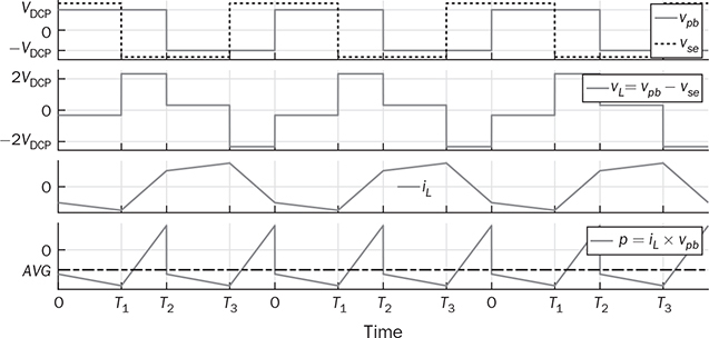
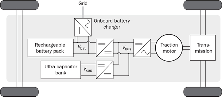
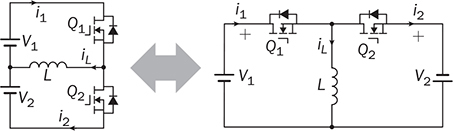
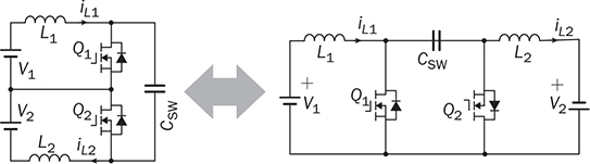
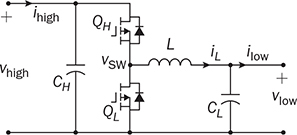
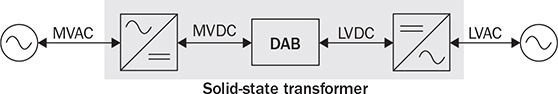
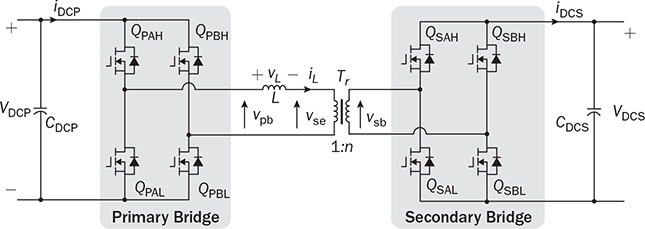
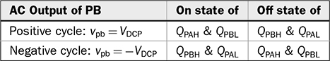
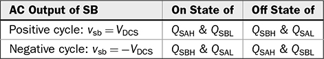
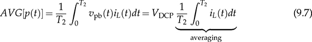
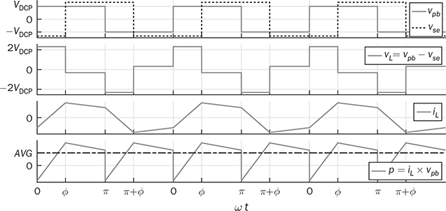
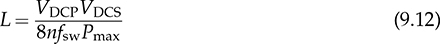
The discussion in previous chapters focused on the unidirectional converters. The power source and load can be clearly distinguished to identify the active power flow direction. According to the classification in Sec. 1.1, another group of power conversion is bidirectional, applications of which are increasing because of the large utilization of rechargeable batteries for electrical vehicles (EVs) and grid interconnection. Power transformers can support voltage conversion and bidirectional power flow in a passive way. The latest applications are based on power converters to control the bidirectional power flow. Figure 9.1 demonstrates one system configuration to operate an EV. FIGURE 9.1 Diagram example of electric vehicle. When the EV is running at the nominal condition, the power source is the rechargeable battery pack to supply active power to the DC bus, Vbus. The ultracapacitor bank can be discharged to support short-term power in case the vehicle accelerates. The DC/AC stage drives the traction motor to rotate. When the vehicle goes for a long downhill, the motor can become a generator to produce braking power. The regenerated power should be through the AC/DC path and inject to the DC bus. Meanwhile, the battery and ultracapacitor units should be charged via the bidirectional DC/DC converters to store the braking energy. The four power converters shown in Fig. 9.1 shall be bidirectional to operate the EV efficiently. Following the smart grid concept, future EVs should participate in power management and grid support. When a single converter is used for interfacing rechargeable batteries, bidirectional power conversion is required. An equalizing process is generally required to avoid mismatch effect of rechargeable battery cells when a series-connected stack is formed. The series connection of battery cells is utilized in many applications to boost the output voltage, e.g., EV and bulk storage units for grid support. In one string, all battery cells are charged and discharged at the same level of current, which is prone to potential damage or lifetime reduction if nonuniformity exists among cells. Figure 9.2 illustrates one equalization example using power conversion techniques. Only two battery cells are present to simplify the analysis. When the equivalent circuit is derived and plotted, the conversion topology is related to the buck-boost converter. The metal-oxide semiconductor field-effect transistor (MOSFET), Q2, is used to replace the freewheeling diode in the conventional buck-boost converter. Thus, the bidirectional power flow is activated to exchange energy among the battery cells via the interlinking inductor, L. The on-state duty ratio of Q1 determines the power flow direction and level. Another FET, Q2, is complementarily switched to maintain the inductor current flow. When a 50% duty ratio is applied, the terminal voltage of the two battery cells is theoretically the same according to the steady-state analysis of buck-boost converters. If unbalancing happens, the cell with a higher voltage will be discharged and supply power to the lower-voltage cell until a new equalization is reached. FIGURE 9.2 Bidirectional DC/DC for battery equalization by buck-boost topology. The ´ Ćuk converter shares the same voltage conversion ratio as the buck-boost converter in the steady state. The bidirectional version can also be used to equalize battery cells, as illustrated in Fig. 9.3. The passive switch is replaced with an active switch, MOSFET. The capacitor CSW is utilized as the central interlink for energy exchange and power conversion. In theory, the battery terminal voltage in steady state should be the same when a 50% duty cycle is alternatively applied to the two active switches. FIGURE 9.3 Bidirectional DC/DC for battery equalization using ´ Ćuk topology. The synchronous buck converter is widely applied for ELV power interfaces because of the high efficiency and linear voltage conversion ratio in the continuous conduction mode (CCM). The circuit is illustrated in Fig. 9.4, which is constructed by an active two-switch bridge. When the terminal vhigh is connected to the source, the circuit forms a buck converter that allows power flow from the left to the right, where a load is connected. When the terminal vlow is connected to a source, the topology is changed to a boost converter that can supply active power from right to left. FIGURE 9.4 Non-isolated DC/DC converter formed by two active switches. When both sides include sources and loads, the bidirectional power flow can be achieved since both terminals can perform power sink and source. The duty ratio for PWM determines the direction and level of power flow with regards to the steady-state voltage levels of vhigh and vlow. The condition of the bidirectional power flow is that vlow < vhigh in steady state. When vlow ≥ vhigh, the converter is out of control since the antiparallel diode of QH creates a path for direct current flow. One special bidirectional DC/DC topology draws recent attention, which is the dual active bridge (DAB) DC/DC converter. The topology is not new since it was released in 1989 as a US patent, indexed as 5027264. Thyristors were shown in the patent to construct the active bridges. The latest implementations are based on FETs and IGBTs. The topology is flourishing because of features of bidirectional power flow and galvanic isolation. One discussion is about solid-state transformers, which are expected to replace conventional transformers used in AC electric power distribution. Figure 9.5 demonstrates the transformer function linking a LVAC network with the MVAC grid. The power electronic device reduces the size and weight of power transformation and adds controllability to improve AC power systems. The interlink can be achieved by a DAB to serve the functions of voltage conversion, bidirectional power flow, and galvanic isolation. The features also allow the topology to interface rechargeable battery packs, as discussed at the beginning of the chapter. FIGURE 9.5 Dual active bridge used for the internal link solid-state transformers. Figure 9.6 illustrates the circuit of a DAB converter including two active four-switch bridges, shown as the primary bridge (PB) and the secondary bridge (SB). The interlink between the AC ports are the HF transformer, Tr, and the inductor, L. The diagonal switching devices in each bridge are paired and controlled by the same gate signal for on/off to produce either [+] cycle or [−] cycle. The paired switching scheme of the PB and SB is shown in Tables 9.1 and 9.2, respectively. The two active bridges produce high-frequency AC (HFAC) to exchange power through the interlinking transformer and inductor. FIGURE 9.6 Standard circuit of dual active bridge. TABLE 9.1 Paired Switching Scheme of Primary Bridge TABLE 9.2 Paired Switching Scheme of Secondary Bridge In a steady state, the voltages at the DC terminals are steady, shown as VDCP and VDCS. The two active bridges act as DC/AC conversion to produce HFAC voltage signals, vpb and vsb, as shown in Fig. 9.6. The amplitude difference between vsb and vse comes from the winding turns ratio, n. The amplitudes of vpb and vse can be determined as VDCP and VDCS/n, respectively. The key waveforms are demonstrated in Fig. 9.7 for the steady-state analysis. The modulation of DAB produces the same switching frequency of the signals of vpb, vsb, and vse. The inductor voltage depends on the difference of vpb and vse, which is expressed by vL = vpb − vse. The inductor current responds to the crossing voltage and shows FIGURE 9.7 Waveforms of dual active bridge at steady state in time domain. According to the DAB circuit, as shown in Fig. 9.6, the instantaneous power can be expressed by p(t) = vpb(t) × iL(t). Figure 9.7 indicates the repeated cycle of p(t) from 0 to T2. The averaged value of p(t) indicates the direction of the active power in steady state. If the averaged value is positive, AVG[p(t)] > 0, the active power flow is from the PB to the SB. The time difference between vpb and vse is shown as T1, which is constant in the steady state. Due to the interlinking inductance, L, the inductor current is limited by the switching frequency. Since iL is AC and zero-mean in steady state, the signal shows the repeatable sequence with four states, which are divided by the moments, T1, T2, and T3. Regarding the periodic waveform of iL, as shown in Fig. 9.7, the following condition holds: Considering the time period from 0 to T1, the value of iL changes from iL(0) to iL(T1), which is expressed by where VSE is the amplitude of vse and theoretically equal to Following (9.1), (9.3), and (9.4), the initial value of iL can be determined by Substituting iL(0) in (9.3) yields the expression for iL(T1) in (9.6). The four current levels of iL in the steady state become known since iL(T2) = −iL(0) and iL(T3) = −iL(T1). According to Fig. 9.7, the power waveform is repeated for each half cycle, 0–T2. Therefore, the averaged power can be computed by The averaged value of p(t) in a steady state is determined by In the steady state, the DAB signals are periodic, which can also be translated into the phase representation regarding the switching frequency, ω. The phase angle is normalized by following the reference signal of vpb from 0 to 2π, as shown in Fig. 9.8. The time delay, T1, between vpb and vse, as shown in Fig. 9.7, is then equivalent to the phase shift, ϕ = ωT1. The half-cycle period, T2, is expressed by π in the phase representation. Following (9.8), the average power in steady state can be transformed into the expression in phase format. A nonlinear equation is derived as (9.9), which indicates the control variables ϕ and ω. It shows that the power level goes up by a decrease of ω. When ω is fixed for the switching operation, the phase angle ϕ between vpb and vse becomes the main control input to regulate the power flow. FIGURE 9.8 Waveforms of dual active bridge in phase domain. When 0 < ϕ < π, the averaged power is positive in value by following (9.9). When ω is a constant, the averaged power in steady state is a function of the applied phase, ϕ, which can be expressed by pavg(ϕ). The maximum power level can be determined by the partial differentiation, The highest power flow happens in steady state when the control variable is assigned to be where fsw is the frequency of vpb or vsb in hertz and ω = 2πfsw. Following the above steady-state analysis, the design procedure of a DAB follows: 1. Specify the nominal values of VDCP and VDCS. 2. Specify the power rating or the highest power level, Pmax. 3. Decide the proper winding turns ratio, n, based on the ratio of VDCP and VDCS. 4. Specify the switching frequency, fsw, and ω = 2πfsw. 5. Determine the value of the interlinking inductance, L, according to The analysis in Sec. 9.2.1 shows the averaged power value is positive. Modulation can achieve reverse power flow. An example of the reverse power flow is shown in Fig. 9.9, where the averaged power is computed to be negative in value. Regarding the periodic waveform of iL in each switching moment, as shown in Fig. 9.9, the following condition holds: FIGURE 9.9 Waveforms of dual active bridge showing reverse power flow in time domain. Following Fig. 9.9, the value of
CHAPTER9

Bidirectional Power Conversion
9.1 Non-Isolated DC/DC Conversion
9.2 Dual Active Bridge
9.2.1 Forward Power Flow
 . The instantaneous level of nonzero vL leads to the amplitude of iL increasing or decreasing, as illustrated in Fig. 9.7. The signal of iL is AC and indicates the zero mean in each steady-state cycle.
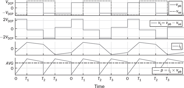


 . From T1 to T2, the inductor current reaches to the new level:


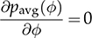 . Following (9.9), the critical phase value that represents the highest power flow is determined by

 . The highest value of the averaged power is expressed by (9.11) to represent the power rating.

9.2.2 Reverse Power Flow