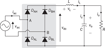
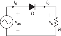
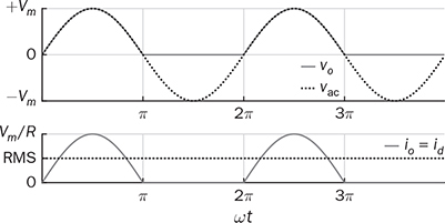
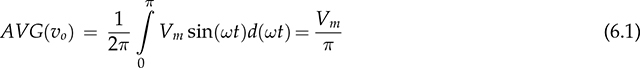
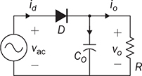
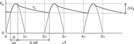
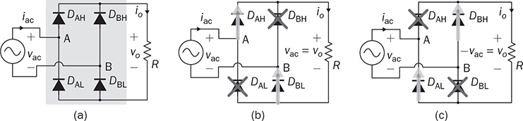
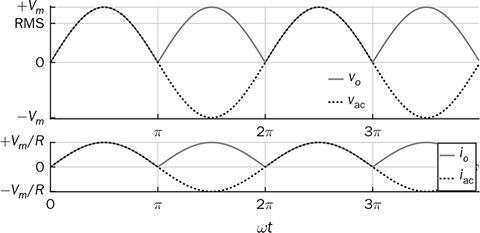
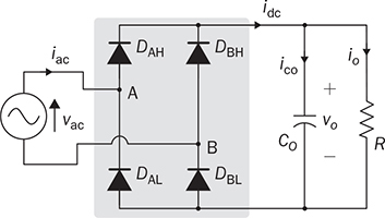
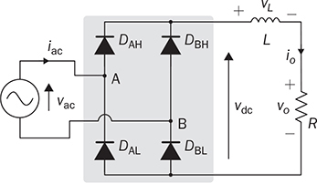
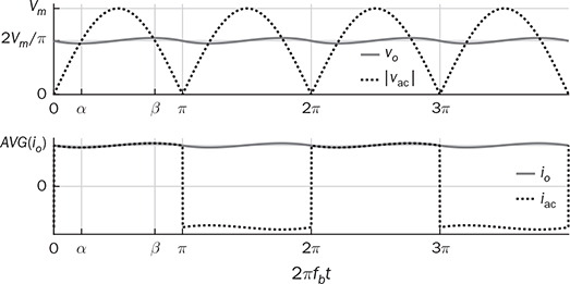
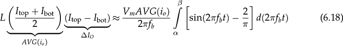
Single-phase AC supplies most homes and offices due to relatively low power demand and simple wiring. Since more and more devices are DC-based, the AC/DC conversion is required. The AC/DC conversion and converter are commonly called as the rectification and rectifier, respectively. Diodes automatically pass forward current and block reverse current. The feature of one-direction conduction supports circuit constructions for the AC/DC conversion. Figure 6.1 shows a simple rectifier using only one diode. The topology is named as the half-wave rectifier since only the positive cycle of vac can appear at the output terminal and supply the load. The AC source voltage is expressed as vac = Vm sin(ωt). The input current passes through the diode and becomes the same as the output, id = io, as shown in Fig. 6.2. The average voltage of the output can be determined by (6.1), the RMS value is derived by (6.2), and the averaged power is computed by (6.3). The output voltage and current are discontinuous when a pure resistive load is applied at the output terminal. The power quality is considerably low at both the input and output port. The power factor for the AC side can be computed as 0.707. Following the DC quality discussion in Sec. 4.6, the form factor of vo is 0.637, which is also low. FIGURE 6.1 Half-wave rectifier circuit using one diode. FIGURE 6.2 Waveforms of half-wave rectifier circuit. To improve the DC quality of vo and io, capacitors can be applied in parallel with the load, as illustrated in Fig. 6.3. The capacitor, CO, is expected to smoothen the DC voltage, vo. The diode is conducting and connect the source only if the instantaneous value of vac is higher than vo. The time period refers to as “D on,” as illustrated in Fig. 6.4. The voltage of vo follows the same as the Vm sin(ωt) during the on-state of the diode. The diode is naturally turned off by the reverse-bias condition when vac = Vm sin(ωt) < vo. During the off-state, the capacitor CO is discharged by load power consumption, which leads vo to decrease. The peak-to-peak voltage ripple is ΔVO, as indicated in Fig. 6.4. The averaged value of vo can be approximated by FIGURE 6.3 Half-wave rectifier with C filtering. FIGURE 6.4 Waveforms of half-wave rectifier circuit with C filter. When ΔVO is assigned to be low enough, the conduction time of D is much shorter than the off-state period. The diode is reverse-biased and off-conducting for most of the line cycle, as illustrated in Fig. 6.4. When the off-state of D is approximated as the whole line cycle, the following can be established: According to (6.5), the capacitance can be sized for CO when ΔVO is specified, as expressed by where fb is the fundamental frequency of vac, ω = 2πfb. A case study can demonstrate the design of a half-wave rectifier. The input voltage, vac, is rated as 230 V for the RMS value with a frequency of 50 Hz. The averaged value of the output voltage is specified as 320-V DC without any loss consideration. The load resistance is rated by R = 1024 Ω. Following (6.4), the peak-to-peak ripple of the output voltage, ΔVO, can be approximated to be 10.54 V. The capacitance at the DC side can be rated as CO = 593 μF by (6.6). Significant capacitance is generally required to maintain the output voltage with low ripples for high power ratings due to the half-cycle conduction. Figure 6.5a illustrates the passive four-switch bridge used for single-phase AC to DC conversion. For the positive half-cycle of the input voltage (vac), the diagonal pair of DAH and DBL are forward-biased, as illustrated in Fig. 6.5b. The current flow is from DAH to R and then DBL for returning to the source. Meanwhile, another diagonal pair of DBH and DAL are reverse-biased. When the negative half-cycle of the input voltage (vac) appears, the diagonal pair of DBH and DAL are forward-biased, as illustrated in Fig. 6.5c. The current flow is from DBH to R and then DAL for return. The output voltage is always positive regardless of the polarity of vac, which gains the name of full-wave rectification. FIGURE 6.5 Full-wave rectifier for single-phase AC to DC conversion: (a) circuit; (b) positive cycle; (c) negative cycle. Considering ideal diodes, the waveforms of voltage and current are illustrated in Fig. 6.6. The DC voltage, vo, is continuous and repeats the same every half of the line cycle. The double-line frequency appears at vo, which is equal to 2ω, corresponding to the definition, vac = Vm sin(ωt). The average voltage of the output can be derived in (6.7). Furthermore, the RMS value can be computed by (6.8), the same RMS value of vac without consideration of any non-ideal factors. The input AC signals, vac and iac, are in phase and show unity power factor without distortion. Without filtering, the output power quality is low for DC loads since the peak-to-peak ripple is equal to Vm. The form factor is derived to be FIGURE 6.6 Waveform of full-wave rectifier in operation with resistive loads. A capacitor can be implemented across the load to improve the quality of vo, as shown in Fig. 6.7. The circuit operation is commonly called the peak detection since the diodes conduct only if |vac| > vo. The operation principle is simple by following the diode I-V characteristics, and can be described by the following: FIGURE 6.7 Circuit of full-wave rectifier in operation with C and R. • When vac > vo, the diagonal diode pair, DAH and DBL, conducts. • When −vac > vo, the diagonal diode pair, DBH and DAL, conducts. • When |vac| > vo, one diagonal diode pair is forward-biased; CO is charged and load is supplied by the AC source. • When |vac| ≤ vo, all diodes are reverse-biased to isolate the load from the source; CO is discharged to keep vo steady. When a significant volume of CO is considered, the operation of the peak detection is as illustrated in Fig. 6.8. The waveform of vo is close to a straight line and rides on the top of |vac|. When all diodes are reverse-biased, the AC source is disconnected from the load. The right side becomes a simple RC circuit that the capacitor, CO, is discharged to slow down the voltage drop of vo, as shown by the zoom-in plot in Fig. 6.8. The condition can be expressed by FIGURE 6.8 Voltage waveform of full-wave rectifier in operation with C filtering. where TOFF refers to the period of the off-state, and ΔVO represents the voltage drop of vo from top to bottom in each half cycle, as illustrated in Fig. 6.8. The averaged value of vo can be estimated by (6.10). When the value of AVG(vo) is specified, the peak-to-peak voltage ripple can be determined by (6.11). One important approximation is made that the off-state period is the half cycle, as expressed by FIGURE 6.9 Waveform of full-wave rectifier in operation with C filtering. where the voltage source is vac = Vm sin(2πfbt). A case study can demonstrate the design of a full-wave rectifier with C filtering, as shown in Fig. 6.7. The input voltage, vac, is rated by 230 V (RMS) and 50 Hz (frequency). The averaged value of the output voltage is specified as 320-V DC without any loss consideration. The load resistance is rated by R = 1024 Ω. The specification is the same as the case study for the half-wave rectifier for comparison. Following (6.11), the peak-topeak ripple of the output voltage, ΔVO, can be approximated as 10.54 V. The capacitance at the DC side can be rated as CO = 297 μF by (6.12). Distortion at the DC waveform can be reduced by other smoothing components, i.e., inductors. When an inductor is in series with the load resistor, as shown in Fig. 6.10, the current, io, is expected to be smooth according to (6.13). FIGURE 6.10 Circuit of full-wave rectifier in operation with LR. where vac = Vm sin(2πfbt). When |vac| > vo, the inductor current rises according to (6.13). Otherwise, the level of io reduces if |vac| < vo. The steady-state waveform is illustrated in Fig. 6.11, showing low ripples of vo. The average voltage across L is zero in steady state; therefore, the averaging value of vo can be derived as the same result as expressed in (6.7) without loss consideration. The average value of io can be determined by (6.14). When L is significant in value, the waveform of vo is flat, represented by the averaged value of vo, AVG(vo). Thus, the energy is stored in L and leads to the rise of io from bottom to top, which is expressed by (6.15). FIGURE 6.11 Waveform of full-wave rectifier with L filtering. where Itop and Ibot refer to the highest and lowest value of io in a steady state; Ttop and Tbot indicate the moment when io = Itop and io = Ibot, respectively. The moment of Ttop and Tbot can be identified as the phase representation as α and β, which is shown in Fig. 6.13 and can be identified by A further derivation leads to (6.18) and (6.19). The rating of L can be determined by (6.19) when the peak-to-peak current ripple, ΔIO, is specified. The ripple percentage of the current is the same as the relative ripple level of vo when the resistive load is applied. A case study can demonstrate the design of a full-wave rectifier with L filtering. The input voltage, vac, is rated as 230 V (RMS) and 50 Hz (frequency). The nominal load resistance is rated as R = 20.71 Ω. The averaging values of vo and io in the steady state are specified to be 207.1 V and 10 A, respectively. When the peak-to-peak ripple of io is designed to be ΔIO = 20% × AVG(io), the same percentage value is applied to the voltage ripple of vo. The inductance can be determined by (6.19) to be L = 218 mH. In general, the higher the L, the flatter the values of io and vo that can be achieved. The filtering aims to improve the power quality of the DC current output but leads to the concern of the power quality of the input current. As shown in Fig. 6.11, the waveform of iac is seriously distorted from the sinusoidal format. A high level of THD can be expected to measure the waveform of iac. When L is significantly high in value, the waveform of iac is close to a square waveform. Figure 6.12 demonstrates the single-phase AC to DC conversion, including an LC filter. The integration is effective since the capacitor maintains the crossing voltage, and the inductor smoothens the through current. The four-switch bridge of diodes only allows vdc ≥ 0. Therefore, the inductor current can be with either a continuous conduction mode (CCM) or discontinuous conduction mode (DCM). The definitions of CCM and DCM are the same as provided in Chap. 3. FIGURE 6.12
CHAPTER 6

Single-Phase AC to DC Conversion
6.1 Half-Wave Rectification


6.1.1 Capacitor for Filtering


6.1.2 Case Study
6.2 Full-Wave Bridge Rectifier
 which clearly shows better DC quality than the half-wave rectifier.


6.2.1 Capacitor for Filtering
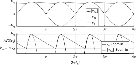


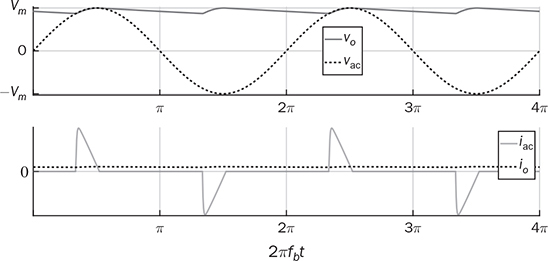
 . Following (6.9) and the low ripple of vo, the output capacitor can be rated by (6.12). When the capacitance is significant, the output DC voltage is maintained in good quality. However, the main issue is from the quality of the input current, iac, as illustrated in Fig. 6.9. It shows a significantly high current peak in comparison with the load current, io, to balance the power flow from AC to DC. The diodes conduct current only for a short time within each half-cycle. The distorted waveform of iac is measured to be more than 100% in total harmonic distortion (THD). Without additional power factor correction, the C-type filter and the peak detection operation can only qualify for low-power applications to avoid significant disturbance to power grids.
6.2.2 Inductor for Filtering


6.2.3 LC Filter