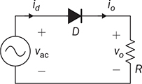
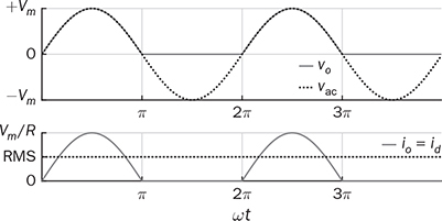
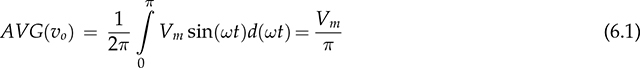
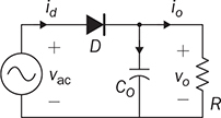
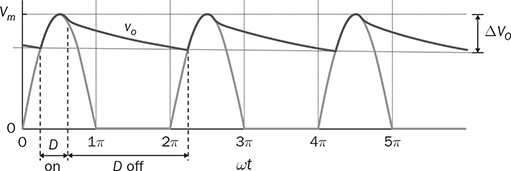
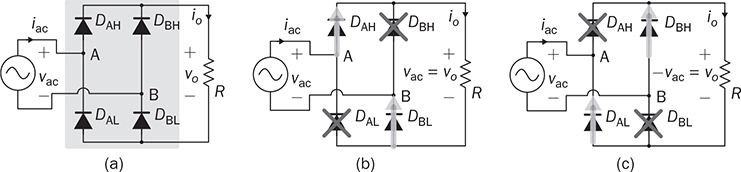
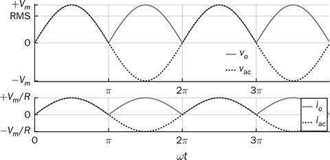
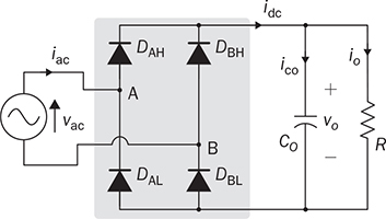
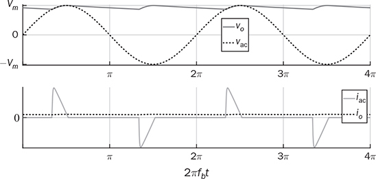
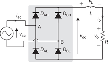
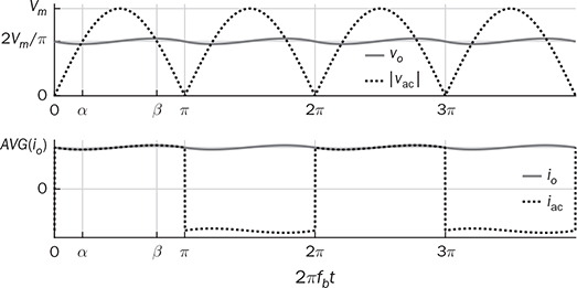
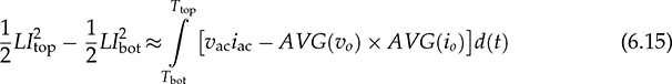
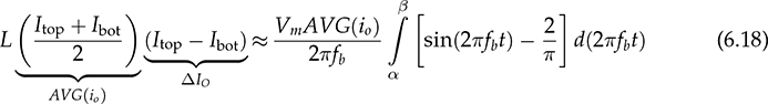
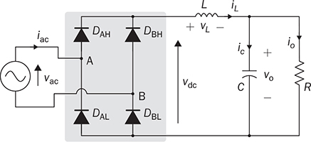
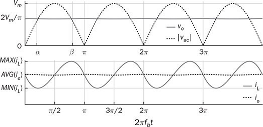
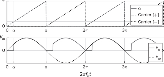
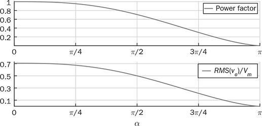
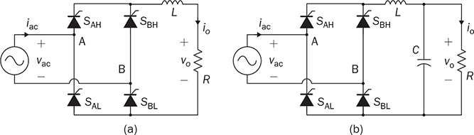
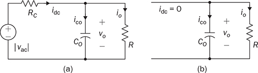
Single-phase AC supplies most homes and offices due to relatively low power demand and simple wiring. Since more and more devices are DC-based, the AC/DC conversion is required. The AC/DC conversion and converter are commonly called as the rectification and rectifier, respectively. Diodes automatically pass forward current and block reverse current. The feature of one-direction conduction supports circuit constructions for the AC/DC conversion. Figure 6.1 shows a simple rectifier using only one diode. The topology is named as the half-wave rectifier since only the positive cycle of vac can appear at the output terminal and supply the load. The AC source voltage is expressed as vac = Vm sin(ωt). The input current passes through the diode and becomes the same as the output, id = io, as shown in Fig. 6.2. The average voltage of the output can be determined by (6.1), the RMS value is derived by (6.2), and the averaged power is computed by (6.3). The output voltage and current are discontinuous when a pure resistive load is applied at the output terminal. The power quality is considerably low at both the input and output port. The power factor for the AC side can be computed as 0.707. Following the DC quality discussion in Sec. 4.6, the form factor of vo is 0.637, which is also low. FIGURE 6.1 Half-wave rectifier circuit using one diode. FIGURE 6.2 Waveforms of half-wave rectifier circuit. To improve the DC quality of vo and io, capacitors can be applied in parallel with the load, as illustrated in Fig. 6.3. The capacitor, CO, is expected to smoothen the DC voltage, vo. The diode is conducting and connect the source only if the instantaneous value of vac is higher than vo. The time period refers to as “D on,” as illustrated in Fig. 6.4. The voltage of vo follows the same as the Vm sin(ωt) during the on-state of the diode. The diode is naturally turned off by the reverse-bias condition when vac = Vm sin(ωt) < vo. During the off-state, the capacitor CO is discharged by load power consumption, which leads vo to decrease. The peak-to-peak voltage ripple is ΔVO, as indicated in Fig. 6.4. The averaged value of vo can be approximated by FIGURE 6.3 Half-wave rectifier with C filtering. FIGURE 6.4 Waveforms of half-wave rectifier circuit with C filter. When ΔVO is assigned to be low enough, the conduction time of D is much shorter than the off-state period. The diode is reverse-biased and off-conducting for most of the line cycle, as illustrated in Fig. 6.4. When the off-state of D is approximated as the whole line cycle, the following can be established: According to (6.5), the capacitance can be sized for CO when ΔVO is specified, as expressed by where fb is the fundamental frequency of vac, ω = 2πfb. A case study can demonstrate the design of a half-wave rectifier. The input voltage, vac, is rated as 230 V for the RMS value with a frequency of 50 Hz. The averaged value of the output voltage is specified as 320-V DC without any loss consideration. The load resistance is rated by R = 1024 Ω. Following (6.4), the peak-to-peak ripple of the output voltage, ΔVO, can be approximated to be 10.54 V. The capacitance at the DC side can be rated as CO = 593 μF by (6.6). Significant capacitance is generally required to maintain the output voltage with low ripples for high power ratings due to the half-cycle conduction. Figure 6.5a illustrates the passive four-switch bridge used for single-phase AC to DC conversion. For the positive half-cycle of the input voltage (vac), the diagonal pair of DAH and DBL are forward-biased, as illustrated in Fig. 6.5b. The current flow is from DAH to R and then DBL for returning to the source. Meanwhile, another diagonal pair of DBH and DAL are reverse-biased. When the negative half-cycle of the input voltage (vac) appears, the diagonal pair of DBH and DAL are forward-biased, as illustrated in Fig. 6.5c. The current flow is from DBH to R and then DAL for return. The output voltage is always positive regardless of the polarity of vac, which gains the name of full-wave rectification. FIGURE 6.5 Full-wave rectifier for single-phase AC to DC conversion: (a) circuit; (b) positive cycle; (c) negative cycle. Considering ideal diodes, the waveforms of voltage and current are illustrated in Fig. 6.6. The DC voltage, vo, is continuous and repeats the same every half of the line cycle. The double-line frequency appears at vo, which is equal to 2ω, corresponding to the definition, vac = Vm sin(ωt). The average voltage of the output can be derived in (6.7). Furthermore, the RMS value can be computed by (6.8), the same RMS value of vac without consideration of any non-ideal factors. The input AC signals, vac and iac, are in phase and show unity power factor without distortion. Without filtering, the output power quality is low for DC loads since the peak-to-peak ripple is equal to Vm. The form factor is derived to be FIGURE 6.6 Waveform of full-wave rectifier in operation with resistive loads. A capacitor can be implemented across the load to improve the quality of vo, as shown in Fig. 6.7. The circuit operation is commonly called the peak detection since the diodes conduct only if |vac| > vo. The operation principle is simple by following the diode I-V characteristics, and can be described by the following: FIGURE 6.7 Circuit of full-wave rectifier in operation with C and R. • When vac > vo, the diagonal diode pair, DAH and DBL, conducts. • When −vac > vo, the diagonal diode pair, DBH and DAL, conducts. • When |vac| > vo, one diagonal diode pair is forward-biased; CO is charged and load is supplied by the AC source. • When |vac| ≤ vo, all diodes are reverse-biased to isolate the load from the source; CO is discharged to keep vo steady. When a significant volume of CO is considered, the operation of the peak detection is as illustrated in Fig. 6.8. The waveform of vo is close to a straight line and rides on the top of |vac|. When all diodes are reverse-biased, the AC source is disconnected from the load. The right side becomes a simple RC circuit that the capacitor, CO, is discharged to slow down the voltage drop of vo, as shown by the zoom-in plot in Fig. 6.8. The condition can be expressed by FIGURE 6.8 Voltage waveform of full-wave rectifier in operation with C filtering. where TOFF refers to the period of the off-state, and ΔVO represents the voltage drop of vo from top to bottom in each half cycle, as illustrated in Fig. 6.8. The averaged value of vo can be estimated by (6.10). When the value of AVG(vo) is specified, the peak-to-peak voltage ripple can be determined by (6.11). One important approximation is made that the off-state period is the half cycle, as expressed by FIGURE 6.9 Waveform of full-wave rectifier in operation with C filtering. where the voltage source is vac = Vm sin(2πfbt). A case study can demonstrate the design of a full-wave rectifier with C filtering, as shown in Fig. 6.7. The input voltage, vac, is rated by 230 V (RMS) and 50 Hz (frequency). The averaged value of the output voltage is specified as 320-V DC without any loss consideration. The load resistance is rated by R = 1024 Ω. The specification is the same as the case study for the half-wave rectifier for comparison. Following (6.11), the peak-topeak ripple of the output voltage, ΔVO, can be approximated as 10.54 V. The capacitance at the DC side can be rated as CO = 297 μF by (6.12). Distortion at the DC waveform can be reduced by other smoothing components, i.e., inductors. When an inductor is in series with the load resistor, as shown in Fig. 6.10, the current, io, is expected to be smooth according to (6.13). FIGURE 6.10 Circuit of full-wave rectifier in operation with LR. where vac = Vm sin(2πfbt). When |vac| > vo, the inductor current rises according to (6.13). Otherwise, the level of io reduces if |vac| < vo. The steady-state waveform is illustrated in Fig. 6.11, showing low ripples of vo. The average voltage across L is zero in steady state; therefore, the averaging value of vo can be derived as the same result as expressed in (6.7) without loss consideration. The average value of io can be determined by (6.14). When L is significant in value, the waveform of vo is flat, represented by the averaged value of vo, AVG(vo). Thus, the energy is stored in L and leads to the rise of io from bottom to top, which is expressed by (6.15). FIGURE 6.11 Waveform of full-wave rectifier with L filtering. where Itop and Ibot refer to the highest and lowest value of io in a steady state; Ttop and Tbot indicate the moment when io = Itop and io = Ibot, respectively. The moment of Ttop and Tbot can be identified as the phase representation as α and β, which is shown in Fig. 6.13 and can be identified by A further derivation leads to (6.18) and (6.19). The rating of L can be determined by (6.19) when the peak-to-peak current ripple, ΔIO, is specified. The ripple percentage of the current is the same as the relative ripple level of vo when the resistive load is applied. A case study can demonstrate the design of a full-wave rectifier with L filtering. The input voltage, vac, is rated as 230 V (RMS) and 50 Hz (frequency). The nominal load resistance is rated as R = 20.71 Ω. The averaging values of vo and io in the steady state are specified to be 207.1 V and 10 A, respectively. When the peak-to-peak ripple of io is designed to be ΔIO = 20% × AVG(io), the same percentage value is applied to the voltage ripple of vo. The inductance can be determined by (6.19) to be L = 218 mH. In general, the higher the L, the flatter the values of io and vo that can be achieved. The filtering aims to improve the power quality of the DC current output but leads to the concern of the power quality of the input current. As shown in Fig. 6.11, the waveform of iac is seriously distorted from the sinusoidal format. A high level of THD can be expected to measure the waveform of iac. When L is significantly high in value, the waveform of iac is close to a square waveform. Figure 6.12 demonstrates the single-phase AC to DC conversion, including an LC filter. The integration is effective since the capacitor maintains the crossing voltage, and the inductor smoothens the through current. The four-switch bridge of diodes only allows vdc ≥ 0. Therefore, the inductor current can be with either a continuous conduction mode (CCM) or discontinuous conduction mode (DCM). The definitions of CCM and DCM are the same as provided in Chap. 3. FIGURE 6.12 Circuit of full-wave rectifier with LC filter. Figure 6.13 illustrates the steady-state waveforms of voltage and current in CCM. The averaged value of vo is determined by (6.7) to be a fixed value of FIGURE 6.13 Waveform of full-wave rectifier with LC filtering. The rise or drop of vo depends on the difference between iL and io, as shown in Fig. 6.14. During the period that the instant value of iL is higher than io, ic = iL − io > 0, thus, the surplus energy charges the capacitor, CO, and increases vo to form energy storage. Therefore, FIGURE 6.14 Waveform of full-wave rectifier at CCM with LC filtering. where Vtop and Vbot are referred to as the highest and lowest value of vo in steady state; Ttop and Tbot indicate the moments when vo = Vtop and vo = Vbot, respectively. In a steady state, the averaged value of ic is equal to zero. The amplitude is the half of the peak-to-peak ripple of iL, as A case study can demonstrate the design of a full-wave rectifier with LC filtering. The input voltage, vac, is rated as 230 V (RMS) and 50 Hz (frequency). The nominal load resistance is rated by R = 20.71 Ω. Based on CCM, the averaging values of vo and io in nominal condition can be determined as 207.1 V and 10 A, respectively. When the peak-to-peak ripple of iL is specified as ΔIL = 30% × AVGio = 3 A, the inductance can be rated by (6.20) as L = 145 mH. When the peak-to-peak ripple of vo is specified as ΔVO = 1% × AVG(vo) = 2.1 V, the capacitance of CO can be rated by (6.23) as CO = 2.3 mF. When FIGURE 6.15 Waveform of full-wave rectifier at BCM with LC filtering. In the DCM, the inductor current is saturated to zero for a certain moment in each cycle, as shown in Fig. 6.16. The crossing points, indicated by α and β, can be derived as in (6.16) and (6.17), respectively. However, the values depend on the averaged voltage of vo, which is unknown for the DCM. Figure 6.16 shows that the non-zero value of iL starts at the point of α. The level of iL rises until the peak point of β, drops to zero at γ, and then saturates at the zero levels. The variation of the inductor current is expressed by (6.25) and (6.26). FIGURE 6.16 Waveform of full-wave rectifier at DCM with LC filtering. where ω = 2πfb and VO = AVG(vo). Therefore, At ωt = γ, the inductor current, iL, reaches the zero level. The condition is expressed by The averaged value of iL is equal to that of io. Thus, the equivalence leads to (6.28) and then (6.29). The unknowns of α, γ, and VO can be identified by the three constraints in (6.16), (6.27), and (6.29). The solution can be achieved by a numerical solver such as “solve” or “fsolve”, in MATLAB. Following the case study discussed earlier in this section, the load condition is changed to R = 552 Ω > Rcrit, which leads to the DCM. Through the numerical solver, “fsolve”, the values of α, γ, and VO can be identified as 0.91 rad, 2.92 rad, and 257.545 V, respectively. The output voltage becomes higher than that of the CCM. The analysis will be verified by the time-domain simulation in Sec. 6.5. The previous implementation of the single-phase AC to DC conversion was based on the passive switches—diodes. The output DC voltage is out of control, which is clamped by the input AC voltage and circuit design. When diodes are replaced with active switching elements, thyristors, the chopping function can scale down the output DC voltage and add controllability. Figure 6.17 illustrates the four-switch bridge that is constructed by thyristors instead of diodes. The definition is available in Sec. 2.3.4. FIGURE 6.17 Full-wave rectifiers constructed by thyristors. A SCR can delay current conduction even through it is forward-biased. Fire angle (α) can be applied to control the delay and limit the conduction time in each half-cycle, as illustrated in Fig. 6.18. The chopping period can step down the voltage level at the output terminal and reach the desired value. The operation is also called the phase control. Modulation is required to produce the dedicated chopping time within each line cycle. Figure 6.18 demonstrates one solution that delivers two sawtooth carriers for the positive and negative cycles. The signals increase from the zero crossings and reset to zero at the end of the half-cycles. The phase delay is introduced and represented by the value of α. When α < Carrier, the modulation outputs fire signals to activate one pair of SCRs for conducting. SCRs in the bridge turn off at every zero crossing. A chopped waveform of vo is produced as shown in Fig. 6.18. The averaged and RMS values of the output voltage can be determined by (6.30) and (6.31), respectively. FIGURE 6.18 Waveform of SCR-based rectifier bridge for voltage regulation. where vac = Vm sin(2πfbt). The chopping operation results in distortion of the input current, iac, and raises the concern of the power quality. The total power factor (PF) is expressed by (4.20), which can be applied to measure the power quality level. Following (6.31) and (4.20), the total PF value is expressed by (6.32) as a function of α. The chopping operation affects the PF at the AC input terminal even with pure resistive load and ideal switches. The PF is plotted according to the firing angle (α), as illustrated by the plot in Fig. 6.19. With the increasing value of α, the PF becomes lower. The angle also affects the voltage conversion ratio, as expressed in (6.31) and illustrated in Fig. 6.19. FIGURE 6.19 Impact of the chopping angle, α. The above discussion is based on the simplest case of the active rectification without any filtering implementation. Figure 6.20 shows the active rectifiers with the filtering circuits using L and LC, respectively. FIGURE 6.20 Active rectifiers with (a) L filter; (b) LC filter. A case study can demonstrate the design of an active rectifier, as shown in Fig. 6.17. The input voltage, vac, is rated as 230 V (RMS) and 50 Hz (frequency). The averaged value of the output voltage shall be controlled to be 120-V DC. The nominal load resistance is rated by R = 10 Ω. The fire angle can be determined by (6.30) to be 80.85°. The RMS values of vo can be determined by (6.31) as 178.28 V and resulted in the power consumption of 3178 W in nominal condition. The total PF of the AC side can be estimated to be 0.7751. The four-diode bridge is simple and reliable, which is widely used. The alternative configuration is available for single-phase AC to DC conversion. When the bridge diodes are replaced by power metal-oxide semiconductor field effect transistors (MOSFETs), the synchronous rectification is realized, as shown in Fig. 6.21. MOSFETs support the current flow from the source terminal to the drain, which are different from other transistors. Modulation is required to activate one pair of MOSFETs synchronized with the forward-biased diodes. It shows the potential to improve the conversion efficiency with the assumption that the conduction loss caused by the Rds(on) of the FETs is lower than that of the voltage drop of the associated antiparallel diode. Therefore, the synchronous rectification is commonly applied for extra-low voltage (ELV) circuits where the voltage drops of diodes become outstanding. Switching loss can be neglected since the switching synchronous generally supports soft switching. FIGURE 6.21 Synchronous rectifier for single-phase AC to DC conversion. The single-phase AC to DC conversion is often configured with a voltage transformer to increase voltage conversion ratios. When a center-tapped transformer is available, the AC/DC conversion can be constructed to achieve the full-wave rectification without applying the four-switch bridge, as shown in Fig. 6.22. The zero voltage potential is assigned at the center tap of the transformer. The positive half-cycle of vac is across the load through the diode, DP, as shown in Fig. 6.22a. The transformer configuration allows the diode, DN, to be forward-biased when the negative half-cycle of vac is supplied to the transformer. The output voltage is determined by (6.33) for the averaged value, and (6.34) regarding the averaged and RMS value. FIGURE 6.22 Full-wave rectifier using tapped transformer with switches of (a) diodes; (b) SCRs. where n indicates the winding turns ratio and vac = Vm sin(ωt). When SCRs replace the diode to fulfil the rectification, as shown in Fig. 6.22b, the output voltage can be regulated by the chopping operation. SCRs can delay the conduction even forward-biased. The averaged level and RMS value of the DC output voltage corresponding to the phase angle, α, become as in (6.35) and (6.36), respectively. where α indicates the applied phase delay for voltage regulation. One advantage of the solution lies in the flexibility of the voltage conversion ratio, because of the winding turns ratio of the center-tapped transformer. Furthermore, the switch count is reduced by half in comparison with the four-switch bridge solution. Finally, the conduction loss of diodes or SCRs can be theoretically reduced by half in comparison with that of the four-switch rectifier bridge. The representation in Fig. 6.22 refers to the simplest cases of the two-switch rectification and two-winding transformer. Multi-winding transformers can be configured to support multiple and different DC voltage outputs. Low-pass filtering, such as C, L, and LC circuits, can be applied to the DC side to improve the DC power quality. The analysis can follow the same procedure discussed in previous sections for the four-switch bridge with the additional consideration of the winding turns ratio, n. This section discusses how to develop simulation models for different rectification approaches, including the half-wave and full-wave rectifiers. The simulation model considers an option to include non-ideal factors of the forward voltage drop within diodes. Figure 6.23 shows the one-diode rectifier for simulation modeling. The equivalent series resistor is introduced, which is symbolized by RC. The resistance is one factor to limit the inrush current during each transition of the diode on/off states. Therefore, the circuit dynamics can be expressed by (6.37). The diode current, id, is discontinuous due to the short-term conduction of the diode in each line cycle, as discussed in Sec. 6.1.1. The id can be modeled and determined by (6.38), considering the forward voltage drop of the diode, VDROP. FIGURE 6.23 Circuit of one-diode rectifier for simulation modeling. A Simulink model can be accordingly constructed to represent the conversion operation, as illustrated in Fig. 6.24. The model inputs include the AC source voltage, vac, and the load current, io. The model outputs include the output voltage, vo, and the diode current, id. The current value of io depends on the output voltage, vo, and the load profile. For a resistive load, the current is determined by FIGURE 6.24 Simulink model of full-wave rectifier with C filter. Simulation can verify the analysis of the case study discussed at the end of Sec. 6.1.1. Figure 6.25 demonstrates the simulated waveforms without considering the forward voltage drop of the diode. The averaged voltage of vo is measured to be 320.3 V with the peak-to-peak ripple of about 10 V. The averaged value is slightly higher than the specification due to the approximation in the design stage. The rating of CO results from the approximation that the off-state time of D is based on the whole line cycle. The diode current, id, shows short conducting in each line cycle. High current peaks show up since the setting of Rc is estimated to be 10 mΩ. FIGURE 6.25 Simulation result of one-diode rectifier with C filter. The full-wave rectifier has been discussed and shown in Fig. 6.5 when filtering is not considered. According to the principle of four-diode bridges, the Simulink model can be constructed to represent a full-wave rectifier, as shown in Fig. 6.26. The AC source voltage is the input shown as vac. The voltage drop of two diodes can be programmed inside the block of “V_drop”, which is formulated by the Simulink block of “dead zone.” Due to the paired operation of the diodes, the bridge is on-state only if |vac| > 2VDROP, where VDROP is the forward voltage of each diode. Otherwise, the conduction of current will halt as the voltage signal is within its deadband. The “ABS” block is used for the rectification from AC to DC following the operation of the diode bridge. The output voltage and current are modeled as the output signals. FIGURE 6.26 Simulink model of one-diode rectifier with C filter. Figure 6.27 demonstrates the simulated result considering the forward voltage of diodes. The case study is based on vac = 12 sin(2πfbt), where fb = 50 Hz. Dead zones can be found in the current waveforms of iac and then io and vo. The load resistance is rated as R = 12 Ω. The forward voltage drop of each diode is 0.5 V. The dead zones and distortion can be found in the waveform of iac, showing the reduced amplitude and deadtime. The THD of iac is measured to be 5.2% in this case study. The dead zone can also be found in the waveforms of vo and io. In this case study, the conduction loss is 0.56 W, resulting in about 10% power loss. The rectification can only achieve the best efficiency of 90%. The distortion and power losses lead to the development of synchronous rectification for ELV power supplies. FIGURE 6.27 Waveform distortion due to diode voltage drop. A full-wave rectifier circuit is shown in Fig. 6.7, where the load is in parallel with the capacitor to smoothen the output voltage. The circuit dynamics can be expressed by (6.39), where idc is discontinuous due to the on/off state of the diodes. Figure 6.28 illustrates the equivalent circuits regarding the on/off operation of diodes. One equivalent series resistor is introduced, which is symbolized by RC. The resistance is one factor to reflect the inrush current when one pair of diodes is suddenly forward-biased. FIGURE 6.28 Equivalent circuits of full-wave rectifier: (a) diode on-state; (b) diode off-state. When the diode voltage drop is neglected and |vac| > vo, one pair of diodes is forward-biased and results in the equivalent circuit, as shown in Fig. 6.28a. The current of idc can be determined by When |vac| ≤ vo, all diodes are reverse-biased, which is shown by the equivalent circuit in Fig. 6.28b. Accordingly, the Simulink model can be built to represent the rectification, as shown in Fig. 6.29. FIGURE 6.29 Simulink model of one-diode rectifier with C filter. The AC signal, vac, is the input of the model. The voltage drop of the diodes is represented by the block of “V_drop”. The “ABS” block represents the rectification from AC to DC. Due to the paired operation of diodes, the bridge is on-state only if |vac| > (vo + 2VDROP), where VDROP is the forward voltage of each diode. The saturation block represents the peak-detection operation. The load condition responds to vo and results in the current, io. The case study in Sec. 6.2.1 is simulated. When the voltage drop of diodes is assigned to be zero, the averaged voltage is shown as 320.5 V with the peak-to-peak ripple of about 10 V, as shown in Fig. 6.30. The averaged value of vo is slightly higher than the specification. The error results from the rating of the capacitor, which is based on the approximation in (6.12). The waveform of iab shows a high peak value, which indicates the short conducting time of diodes around each peak of vac. The peak value results from the setting of Rc, which is 5 mΩ. The THD value of iac is considerably high. FIGURE 6.30 Simulation result of full-wave rectifier with C filter. Section 6.2.2 discussed the configuration using an inductor to smoothen the output current. Following the circuit diagram in Fig. 6.10, the output current is derived and expressed by (6.13). Figure 6.31 demonstrates the model to simulate the rectification. The model takes the signal of vac as the input and outputs the inductor current io. With the load condition, the inductor current results in the terminal voltage and feedback into the model. FIGURE 6.31 Simulink model of full-wave rectifier with L filter. The case study in Sec. 6.2.2 can be simulated to prove the design and modeling effectiveness. First, non-ideal factors are not considered to verify the theoretical analysis. Figure 6.32 illustrates simulated waveforms, where the averaged voltage of vo is indicated as 207.1 V. The averaged current of io is 10 A, showing the peak-to-peak ripple of about 2 A, which agrees with the specification. FIGURE 6.32 Simulation result of full-wave rectifier with L filter. Section 6.2.3 discussed the effectiveness of LC circuit to be used for filtering and achieving high DC quality. The circuit dynamics can be represented by a Simulink model, as shown in Fig. 6.33. The model outputs include the inductor current to check its continuity. The integral block for the inductor current shows the saturation function to represent the feature of diodes and the potential of DCM. Other definitions refer to the circuit diagram, as shown in Fig. 6.12. FIGURE 6.33 Simulink model of full-wave rectifier with LC filter. The CCM case discussed in Sec. 6.2.3 can be simulated to prove the model’s effectiveness. The non-ideal factor is not considered for the initial simulation to verify the theoretical analysis. Figure 6.34 shows the simulation results, which include the waveforms |vac|, vo, iL, and io. The values of AVG(vo), AVG(iL), ΔIL, and ΔVO can be measured from the waveforms. The averaged voltage of vo is indicated as 207.1 V with the peak-to-peak ripple of 2.1 V, which is about 1% of AVG(vo) and agrees with the specification. The averaged values of iL and io are 10 A to reflect the load condition. The peak-to-peak ripple of iL is 3 A, agreeing with the design specification. FIGURE 6.34 Simulation result of full-wave rectifier at CCM with LC filter. When the load condition becomes R = Rcrit = 138 Ω, the BCM operation is expected according to the theoretical analysis. Figure 6.35 illustrates the simulation result, which agrees with the BCM expectation. The inductor current reaches the zero level but shows continuous conduction. The voltage waveforms follow the same definition as the CCM case study. FIGURE 6.35 Simulation result of full-wave rectifier at BCM with LC filter. When R = 552 Ω > Rcrit, the DCM operation is expected according to the early analysis in Sec. 6.2.3. Figure 6.36 shows the simulation results including the waveforms of |vac|, vo, iac, iL, and io. The inductor current saturates at the zero level for a certain time in each line cycle. The averaged value of vo becomes 257.56 V, higher than the case study of CCM. The value agrees with the theoretical analysis at the end of Sec. 6.2.3. The waveform distortion of iac is visible. In general, the time-domain simulation verifies the design for the case study that the LC filtering is applied. FIGURE 6.36 Simulation result of full-wave rectifier at DCM with LC filter. When SCRs are utilized for rectification, the power waveform can be chopped and result in voltage regulation. A simulation model can be built according to the SCR bridge and operated by a phase-control operation to reshape the output voltage waveform. Figure 6.37 shows a simplified Simulink model with the function of phase control for the voltage regulation. The value of the phase delay (α) is compared with the unified carrier signal to produce the firing signal to control SCRs and deliver the rectified voltage to the DC output terminal. The period of zero cycles appears to reflect the phase delay assignment, α. FIGURE 6.37 Simulink model of SCR-based rectifier to support voltage regulation. The case study in Sec. 6.3 can be simulated to prove the theoretical analysis. The simulation result is shown in Fig. 6.38, which doesn’t include non-ideal factors. The voltage waveforms are plotted together to demonstrate the comparison between the input and output. The averaged value of vo is measured to be 120 V, which corresponds to the applied phase angle of 80.85°. Distortion and phase delay can be recognized in the current waveforms of io and iac. The power quality of the input and output is poor for the case study since no PF correction is implemented. FIGURE 6.38 Simulation result of the case study for voltage regulation. The I-V characteristics of diodes naturally fit the function of AC/DC conversion. The single-phase AC to DC conversion can be constructed by one diode, which is called the half-wave rectifier. The solution is simple but shows constraints in terms of power capacity and power quality. The majority of single-phase rectifiers refer to either the four-switch bridge or the two-switch approach integrated with a transform. When a center-tapped transformer is applied, the voltage conversion ratio is more scalable because of the winding turns ratio. Furthermore, both the switch count and diode conduction loss are reduced by half in comparison with the four-switch bridge solution. Even though the SCR bridge can provide voltage regulation for the output, the method generally deteriorates the power quality in both AC and DC sides due to the chopping effect. With the fast development of DC/DC converters, the voltage regulation at the AC/DC conversion stage becomes unnecessary. MOSFETs have been widely used in the rectification circuit to replace diodes for ELV applications. The on/off switching of MOSFETs is synchronized with the diode operation. Thus, the topology is commonly known as the synchronous rectifier. The rectification efficiency can be significantly improved since the modern MOSFET shows lower conduction loss than the diode for ELV systems. The LC circuit is widely used for low-pass and smoothing filters in rectification to achieve high quality. The combination of both inductor and capacitor presents a more effective solution than either the single L or C implementation. The application of passive filtering can improve the quality at the DC side, as discussed in previous sections. The form factor and ripple factor are the measurements of DC quality. However, the source current, iac, is severely distorted. Power factor correction (PFC) is mostly required to work with rectifiers to improve power quality at the AC side. The PFC can be formed by either passive compensation circuits or specially designed converters to achieve high power quality at both input and output sides. 1. D. W. Hart, Power electronics, McGraw-Hill, 2011. 2. W. Xiao, Photovoltaic power systems: modeling, design, and control, 1st ed., Wiley, 2017. 6.1 Follow Sec. 6.5.1 to build your own simulation model for the half-wave rectification with capacitor implementation. Use the case study to verify the model. 6.2 A half-wave rectifier based on Fig. 6.3 shall be designed for the specifications: the input voltage, vac, is rated as 120 V (RMS) and 60 Hz (frequency); the averaged value of the output voltage is specified as 165-V DC without any loss consideration. The load resistance is rated by R = 225 Ω. (a) Estimate the peak-to-peak ripple of the output voltage, ΔVO. (b) Determine the capacitance (CO) used at the DC side. (c) Build your model and simulate the operation if the voltage drop of the diode is rated as 1 V and the ESR of the capacitor is 5 mΩ. 6.3 A full-wave rectifier based on Fig. 6.7 shall be designed for the specifications, in the same way as in the above problem. (a) Estimate the peak-to-peak ripple of the output voltage, ΔVO. (b) Determine the capacitance (CO) used at the DC side. (c) Build your model and simulate the operation and show the waveforms of vo, io, and iac when the voltage drop of the diode is rated as 1 V and the ESR of the capacitor is 5 mΩ. 6.4 A full-wave rectifier based on Fig. 6.10 shall be designed for the specifications: vac is rated as 120 V (RMS) and 60 Hz (frequency); R = 10.8 Ω. The peak-to-peak voltage of vo is 10% of the averaged value. (a) Determine the averaged value and the peak-to-peak voltage ripple of the output voltage, vo. (b) Determine the averaged value and the peak-to-peak current ripple of the output current, io. (c) Determine the inductance used for the current filtering. (d) Build your model and simulate the operation and show the waveforms of vo, io, and iac when the voltage drop of the diode is rated as 1 V. (e) Estimate the THD value of iac. 6.5 A full-wave rectifier based on Fig. 6.12 shall be designed for the specifications: vac is rated as 120 V (RMS) and 60 Hz (frequency); R = 10.8 Ω. The peak-to-peak voltage of vo is 2% of the averaged value. (a) Determine the averaged value and the peak-to-peak voltage ripple of the output voltage, vo, with consideration of the CCM. (b) Determine the averaged value and the peak-to-peak current ripple of the output current, io. (c) When the peak-to-peak ripple of the inductor current is specified as ΔIL = 4 A for the CCM, determine the inductance used for the current filtering. (d) Determine the value of CO to satisfy the specification. (e) Determine the critical load condition for the BCM. (f) Build your model and simulate the operation and show the waveforms of vo, iL, and iac at the nominal condition without considering any loss factors. (g) Estimate the THD value of iac. 6.6 Follow the same design parameters as in the above problem, when the load resistance is changed to 216 Ω. (a) Identify the averaged value of vo. (b) Verify the value by time-domain simulation. 6.7 SCRs can be used to replace diodes for the full-wave bridge rectifier, as shown in Fig. 6.17. The specifications: the input voltage, vac, is rated as 120 V (RMS) and 60 Hz (frequency); the load resistance is rated by R = 10 Ω. The averaged voltage of the output is designed to be 100 V. (a) Determine the phase angle to delay the SCR conduction in each half-cycle. (b) Determine the RMS value of vo. (c) Determine the active power in the nominal load condition. 6.8 Based on the specifications of the previous question, an inductor, L = 100 mH, is added in series with the load, as shown in Fig. 6.20a. (a) Determine the averaged voltage of the output. (b) Build the simulation model and simulate the case with the filtering inductor. (c) Check if the averaged value of vo is the expected value. (d) Check the peak-to-peak ripple of the output voltage. (e) Check the peak-to-peak ripple of the inductor current. 6.9 Based on the specification of the previous question, a LC circuit, L = 100 mH, CO = 220 μF, is introduced for filtering the output, as shown in Fig. 6.20b. (a) Determine the averaged voltage of the output. (b) Build the simulation model and simulate the case with the filtering inductor. (c) Check if the averaged value of vo is the expected value. (d) Check the peak-to-peak ripple of the output voltage. (e) Check the peak-to-peak ripple of the inductor current.
CHAPTER 6

Single-Phase AC to DC Conversion
6.1 Half-Wave Rectification


6.1.1 Capacitor for Filtering


6.1.2 Case Study
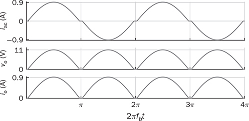
6.2 Full-Wave Bridge Rectifier
 which clearly shows better DC quality than the half-wave rectifier.


6.2.1 Capacitor for Filtering
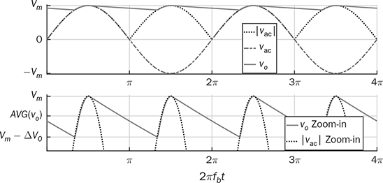


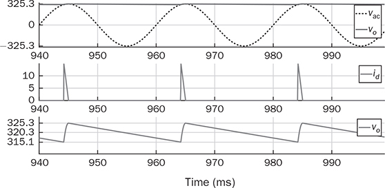
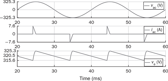
 . Following (6.9) and the low ripple of vo, the output capacitor can be rated by (6.12). When the capacitance is significant, the output DC voltage is maintained in good quality. However, the main issue is from the quality of the input current, iac, as illustrated in Fig. 6.9. It shows a significantly high current peak in comparison with the load current, io, to balance the power flow from AC to DC. The diodes conduct current only for a short time within each half-cycle. The distorted waveform of iac is measured to be more than 100% in total harmonic distortion (THD). Without additional power factor correction, the C-type filter and the peak detection operation can only qualify for low-power applications to avoid significant disturbance to power grids.
6.2.2 Inductor for Filtering


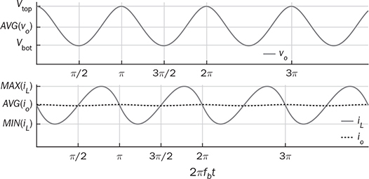
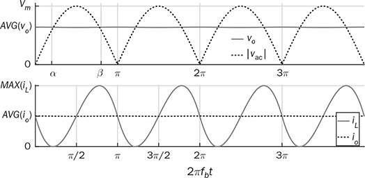
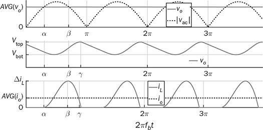
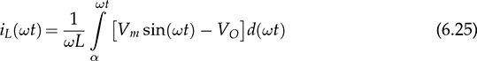
6.2.3 LC Filter
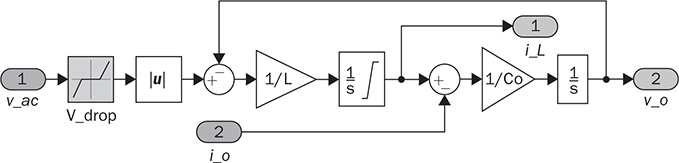
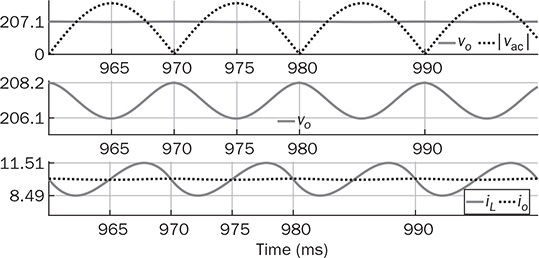
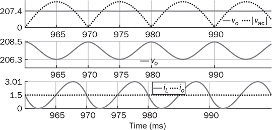
 in theory. Meanwhile, the averaging value of ic is zero in steady state. Therefore, the averaging values of iL and io are the same. The ripple in the DC side follows the frequency, 2fb, which is doubled from the AC frequency since vac = Vm sin(2πfbt). When the LC circuit is sufficiently designed, the waveform of vo is flat and close to the ideal DC signal. The peak-to-peak ripple of iL follows the same analysis from (6.11) to (6.19) in Sec. 6.2.2 and derived as in (6.20). The values of α and β have been identified as 0.22π and 0.78π, as indicated in Fig. 6.13. The inductor can be rated by (6.20) when ΔIL is specified.
 . Therefore, the capacitor current is approximated by ic =
  . The moment of Ttop can be identified as the phase representation as
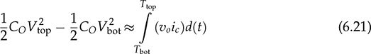
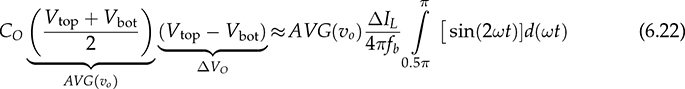
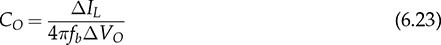
  , which is the beginning of iL > io, as illustrated in Fig. 6.14. The moment of Tbot is referred to as π due to the end of iL > io, which leads to the dropping of vo. The equation in (6.21) can be rewritten as in (6.22). Thus, the capacitance of CO can be rated by (6.23) when the ripples of the inductor current and output voltage are assigned by ΔIL and ΔVO.
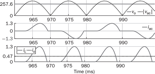
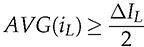 , the inductor current is the CCM. The critical condition is defined by AVG(iL) = ΔIL/2, which is named as the boundary condition mode (BCM). Figure 6.15 demonstrates the waveforms of |vac|, vo, iL, and io at the BCM. The average voltage of vo follows the same as that of the CCM. Thus, the load resistance for the BCM can be determined by (6.24). For the same case study discussed previously, the critical load condition is R = 138 Ω that represents the BCM. When R > Rcrit, the DCM of iL is expected.


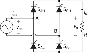
6.3 Active Rectifier

6.4 Alternative Configuration
6.4.1 Synchronous Rectifier
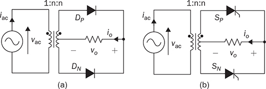
6.4.2 Center-Tapped Transformer


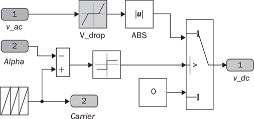
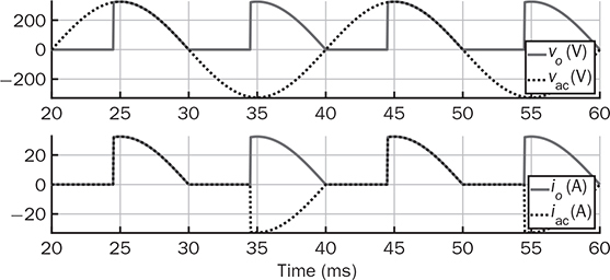
6.5 Modeling for Simulation
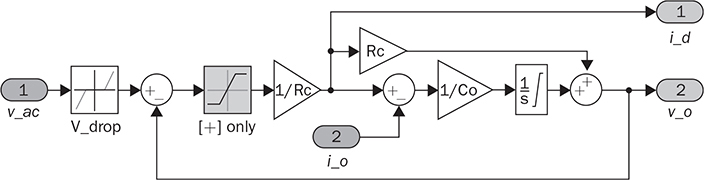
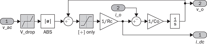
6.5.1 C Filter for One-Diode Rectifier
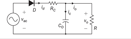

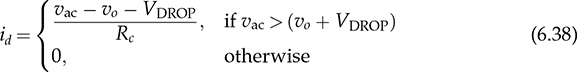
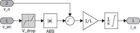
 . The model includes a block of “V_drop”, which is programmable to represent the voltage drop of diodes, VDROP. The saturation block is effective in simulating the operation and computing the value of id, which is expressed by (6.38).
6.5.2 Full-Wave Rectifier without Filtering
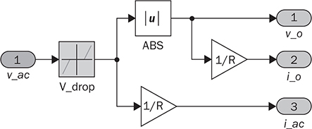
6.5.3 Full-Wave Rectifier with C Filtering


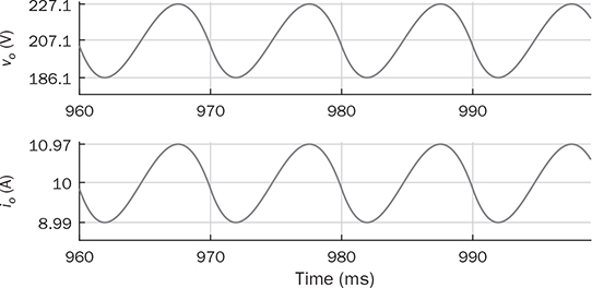
6.5.4 Full-Wave Rectifier with L Filter
6.5.5 Full-Wave Rectifier with LC Filter
6.5.6 Active Rectifier
6.6 Summary
Bibliography
Problems