Abstract
Basic amplifier stages are described in a somewhat cursory fashion. We use circuits that are familiar to most readers and present the analysis in a way that conforms to the estimation analysis described in Chapter 1. This way the reader will encounter familiar calculations in a different framework. The estimation analysis is also applied to nonlinear extensions of the common transfer function expressions. The chapter contains design examples and a set of exercises to ensure that the reader understands the basic concepts.
2.1 Introduction
In this chapter we introduce basic transistor amplifier stages and use them as a starting point to describe the estimation analysis method. For more details on the transistors and the models used we refer to Appendix A.
For the reader familiar with the discussion in books such as [1–5] this chapter should not pose any difficulty.
Fundamentally, all we do in all these simplifications is to linearize the transistor or amplifier at its bias point and draw conclusions about fundamental properties such as gain and impedance. We ignore the body effect for clarity, by assuming that the body is always tied to source in all transistors.
In addition, we will also venture into the world of weak nonlinear effects and show how these gain stages can be analyzed with simple extensions to the standard linearization techniques, all in line with the estimation analysis method.
We start the chapter with a section on single transistor gain stages and continue with a few well-known two transistor stages. For brevity, we will focus on CMOS transistors, but other transistor types such as bipolar can easily be analyzed in the same way. We go through some design examples in detail in order to use the results in the later chapters.
2.2 Single Transistor Gain Stages
Single CMOS transistor gain stages are traditionally divided into three groups: common gate (CG), common drain (CD), and common source (CS) stages. The word common refers to the terminal that is common to both input and output signals, which can be either voltage or current. We will describe them one by one in this section. We will keep the discussion at a general level; the precise expression for the currents’ dependence on terminal voltages does not matter. Only in the final expression, when we are after something specific, do we use specific current voltage relationships described in Appendix A.
CG Stage
The common gate (CG) stage is an amplifier where the gate node is tied to a fixed voltage, possibly with some impedance in series. The input signal enters through the source terminal and exits at the drain terminal. The signal is best described as a current.
Here we will solve for gain and input impedance.
Simplify
We assume the transistor is in saturation so we will ignore the drain gate capacitance. We also assume the drain source impedance is sufficiently large so as not to affect the gain; and finally we assume the output load to be zero ohms. The transistor model in Figure 2.1 shows our assumptions. When comparing with the literature this could be seen as an over-simplification, but we are only interested in the dominant parameters that set the gain and input impedance so that the simplifications are an adequate approximation for an estimation analysis. To calculate the gain we will in addition linearize the transistor around its bias point.
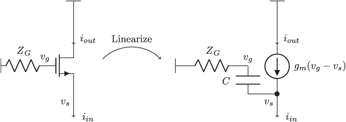
Figure 2.1 Common gate transistor stage with linearization.
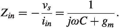
We find for ZG = 0 → vg = 0ZG=0→vg=0 and by applying Kirchoff’s current law (KCL) at the output node
We also know
Solve
By solving for vSvS we find
or
We see for low frequencies that the input current goes straight through to the drain or output, but for higher frequencies the capacitor between the gate and the source will act as a short, effectively grounding the current and leaving nothing to the output. The transition point where |jωC| = gmjωC=gm is a rough estimate of the transition frequency or ftft. A more detailed model can be found in [3]. Here we get
 (2.1)
(2.1)This is an important figure of merit for high speed designs and the expression (2.1) is a convenient rule of thumb.
What about the input impedance? We now have to rewrite iiniin in terms of vsvs:
We find
Imagine now there is a gate impedance, ZGZG. We find
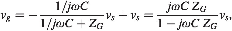
or
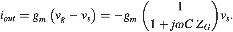
To find the input impedance we need to rewrite iiniin in terms of vsvs.
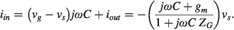
We the find after a simple rearrangement

Verify
As the reader no doubt recognizes, these calculations can be found in any standard electronics book, but here we have made some simplifications beyond that which is normally done. This is all in line with the estimation analysis idea. We are only seeking a model that is simple enough to capture the essence of what we want to know, in this case gain and input impedance. The calculations in this chapter are easy to verify in the literature. We will encounter more complex situations in Chapters 4–7.
Evaluate
We have followed the estimation analysis method and we recognize the calculations from similar examples in the standard literature. To investigate the meaning of these expressions we need to go to various limits of key parameters. This is also often a way to sanity check the answer.
Let us look at the gain

If ω → 0ω→0 we see the gain A → 1A→1. For high frequencies, ω → ∞ω→∞ we see the gain A → 0A→0. Obviously, when gm → 0gm→0 the gain A → 0A→0.
Similarly, for the input impedance

We see an interesting relationship between the gate impedance and its reflection at the source. When ω2π≪ft the gate impedance will be rotated by 90 degrees so a resistor in the gate will look like an inductor at the source, a capacitor will look like a resistor, and, most disturbingly, an inductor will look like a negative resistor, a kind of gain that can cause instabilities. For the limit ω → 0ω→0, the input impedance is simply 1/gm1/gm. In the other limit, ω → ∞ω→∞ the input impedance is simply ZGZG, which makes sense since in this case the gate capacitance shorts the 1/gm1/gm from the transconductor.
CD Stage
For the common drain (CD) stage the input voltage goes to the gate of the transistor and the output is picked off of the source. It is often referred to as a source-follower circuit, or follower for short. The basic circuit configuration can be found in Figure 2.2.

Figure 2.2 Common drain transistor stage with linearization.
We will solve for gain and input impedance.
Simplify
First we will simplify the situation in a similar fashion to the CG stage.
Solve
The output of the source will look like
After a simple rewrite
 (2.2)
(2.2)The input impedance is now calculated by getting the input current

and rearrange to find
 (2.3)
(2.3)Evaluate
Let us look at the expression for gain, equation (2.2). When ω2π≪ft we see

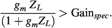
For large load impedances, gmZL ≫ 1 vout → vingmZL≫1vout→vin. In the other extreme, ZL → 0ZL→0 we get vout → 0vout→0, the output is simply shorted to ground.
As in the common gate stage we see the input impedance sees a 90 degree rotation of the impedance at the output, but this time it goes the other way: an inductor looks like a resistor, a capacitor looks like a negative resistor and a resistor looks like a capacitor. In fact for many input stages in narrow-band applications, like cellular phones, this property is a really nice way to create a low-noise input termination with the use of an inductor at the source of the input stage. The input stage will rotate this inductor to look like a real impedance with little noise(!). The remaining capacitor is often resonated out by a series inductor but that is a topic for another book.
CS Stage
The common source stage is perhaps a configuration that one often encounters early on in one’s career. A common setup can be seen in Figure 2.3.

Figure 2.3 Common source transistor stage with output load.
We will calculate gain and input impedance again.
Simplify
The output is a voltage when loaded with an impedance and the input is a voltage. We follow a similar linearization technique to that we had before, but this time we will include the gate drain capacitance, CgdCgd. We then have to solve KCL at the drain and source, we assume the gate driving impedance is zero.
Solve
We have for the basic parameters
We find


Upon substitution of voutvout from the expression of gain above we can rewrite

Verify
As before, this is a standard calculation in [2] but here we made even further simplifications to get an estimate of the gain and impedance.
Evaluate
We see for low frequencies the gain, Again = − gmZLAgain=−gmZL, but there is a cross-over frequency where the gain transitions at ω = gm/Cgdω=gm/Cgd, in effect the major output current is supplied by the gate drain capacitance CgdCgd instead of the transistor gain. In the literature this is known as a right half plane zero. The input impedance is essentially a two-pole system due to the two capacitors. We see for low frequencies the total capacitance is the sum of CC and Cgd(1 + gmZL)Cgd1+gmZL, the gate drain capacitance has been amplified a factor (1 + gmZL)1+gmZL. This effect is known as the Miller effect, the gain across a capacitor will amplify the capacitors value, increasing the effective load.
Nonlinear Extension
We can now employ the same technique to examine nonlinear extensions. In general one needs to employ Volterra series for electronics systems instead of the more commonly known Taylor series. This is due to the fact the systems we are considering have memory in that the output signal depends to some degree on what happened at earlier times in perhaps other parts of the circuit. The simple stages we will look at here have relatively high bandwidth in small geometry CMOS technologies, ft > 100 GHzft>100GHz so we will assume a Taylor series expansion is appropriate. It often turns out to be quite useful, but care must be taken and the important verification step must be completed to make sure we do not fool ourselves and are better served with Volterra series.
For Taylor series we can write the output as a polynomial expansion of the input:

Here

The coefficients can be calculated in several different ways: (1) One can sweep the DC bias point in a simulator and take the appropriate derivatives. (2) One can do a Fourier transform of the output when the input is a single tone sinewave, the linear and higher-order coefficients can be found from the harmonic powers. When relating the two methods keep in mind the mixing effect of the Taylor series when using sinusoids, V0 = A sin ωtV0=Asinωt:

For example, the second-order term splits into a DC component and a second harmonic component. To find the size of the second harmonic term one needs to divide the second-order derivative of the transfer function by a factor of four. A factor of two comes from the Taylor expansion and another factor of two from the mixing action, where half the amplitude goes to DC and rest into the second harmonic. This is similar for higher orders but obviously more complex.
CD Stage
We will follow the CD stage discussion and make a first order correction to the gain calculation.
We start with
where we assume the frequencies of interest are far below ftft, and we are using Figure 2.2 for reference. In this section we limit ourselves to gain calculations.
Simplify
We will first simplify the discussion by assuming the drain source conductance is negligible. We use the following expression for

Finally, the load ZLZL is for this discussion a real impedance.
Solve

We now write

and put this into the expression

Now we identify terms of the same order on each side of the equal sign. We find

We solve for

And finally

Verify
We verify this equation by simply simulating and varying the load, as in Figure 2.4. The basic transistor we are using is biased according to Tables A.2 and A.3 with a resistor at the load in addition to an ideal 1 mA bias current.

Figure 2.4 Simulation setup to verify gain versus load resistance with a fixed bias current.
In effect the current/voltage bias of the transistor is unchanged as we vary the resistive load with its voltage termination so as to not draw additional bias current. We see from Figure 2.5 the agreement is reasonable for small values of the resistance ZLZL but it gets increasingly worse for larger values. The reason for this is the nonlinear impact of the output resistance, roro. In order to improve our predictive power we need to extend the analysis to take this effect into account also as we will show shortly.

Evaluate
We see from the expression something that is somewhat intuitive. By increasing the load impedance we can reduce the effect of the second-order term.
Nonlinear Impact of Output Conductance
The output conductance is modeled as a resistor between source and drain of a transistor.
We will discuss how to calculate gain with this effect in mind.
Simplify
We will extend the analysis to the case where the drain to source conductance is no longer negligible. We have in Figure 2.6 a simplified model where the drain voltage is an AC ground. The capacitance, C, is ignored

Figure 2.6 The output conductance model.
Solve
Here we have the drain current dependent on two voltage differences, vgs = (vg − vs), vds = (vd − vs)vgs=vg−vs,vds=vd−vs. The Taylor expansion of the drain current needs to take both of these voltages into account including all second-order derivatives. We have

The derivatives need to be calculated at the bias point. We can ease the notation by using the following shorthand:

These three quantities can be either estimated or found by sweeping the DC bias point with a simulator. We have now

Using the expressions for vgs, vdsvgs,vds defined above and id = vs/Rlid=vs/Rl we find
 (2.4)
(2.4)We now write

And keeping terms to second order:

We now identify the like terms

We find

Verify
We simulate this situation and find the following comparison graph in Figure 2.7.

We have a much-improved comparison and can feel confident we have the correct model when including the nonlinearity of both the transconductance and output conductance.
Evaluate
It is fairly intuitive to realize the output resistance roro needs to be high to minimize this effect. In a normally biased CMOS transistor gmro ≫ 1gmro≫1, so the impact of a varying output resistance is less significant.
These examples have shown a common situation: one tries to estimate an effect which looks reasonable for certain parameter values but for others it falls short. The task is then to extend the model to cover the greater range by finding out the missing piece. In our case this was relatively simple but other situations can be much more complex. However, the same idea applies: Simplify →→ Solve →→ Verify →→ Evaluate.
CS Stage
The nonlinear extension to the CS stage can be analyzed along the same lines as the CD stage.
Simplify
We make the same simplification as before with

We also ignore all capacitors to make sure the Taylor expansion is valid.
Solve
We write the drain current as

The output voltage is

Thanks to this simple model we now see that we have the nonlinear expression we were looking for.
Verify
This calculation is a trivial extension of the simulation that gives us the expansion parameters in the first place.

Design Examples
We will use our knowledge of the transfer function and impedances of these amplifier stages to build and investigate some real-world examples.
Example 2.1 Estimate input impedance of a CD stage at 25 GHz
In this example we analyze the input impedance of a CD stage with a specific bias and a specific load. The load is another stage which looks capacitive and the interconnect has a, comparatively high, resistance. In effect the load looks like a resistor in series with a capacitor to ground according to Table 2.1. We will use this circuit in Chapter 7.
Table 2.1 Specification table for CD stage
| Specification | Value | comment |
|---|---|---|
| Type | Thin oxide NMOS | |
| Size (W/L/nf) | 1 μm/27 nm/10 | Biased in saturation according to Table A.3 |
| Number of instantiations | 2 | |
| Load | 10 − j/(ω 20 fF)10−j/ω20fF | Ohm |
Solution
We assume the impedance of the current sink bias is large compared to the load impedance in Table 2.1 and we know from equation (2.3), assuming we are far below ftft,

where we have used the definition of ftft.
The operating frequency is about ten times less than ftft (see Appendix A), and we find then

where we have used C = 2 ⋅ 2/3 ⋅ 8 fF ≈ 11 fFC=2⋅2/3⋅8fF≈11fF, which corresponds to a negative resistor with resistance of 3180 ohm and a capacitance of 9 fF at 25 GHz.
Example 2.2 CD stage with resistor capacitor ladder load
In this example we will calculate the transistor size needed to meet a certain output bandwidth. We assume the CD stage gate driving impedance is 0 ohms. The load is here a string of small resistors and at each resistor interconnect there is a capacitor to ground. For details see Table 2.2.
Solution
The load is a series of resistors where at each node connecting the resistors there is a capacitor to ground. The output impedance of the transistor itself is 1/gm1/gm. This impedance will for low frequencies drive the whole capacitive load. At higher frequencies the resistors in the series will eventually dominate the impedance and the gain response will be flat at the transistor source node. We have

Plugging in the numbers we see
We choose our unit transistor, Appendix A, Table A.3, with ten instances in parallel, this results in a current of 10 mA bias. What remains is to estimate the total impedance needed to reach the specified gain. We know the gain from equation (2.2) and with the specification in linear units we find
Where we have assumed ω ≪ ωtω≪ωt. Plugging in the numbers we find

We will require the sink impedance to be larger than 1000 ohms to be on the safe side. The distortion will be small due to this large impedance of the current sink and from the second harmonic terms calculated in the section “Nonlinear Extension: CS Stage” we see the second harmonic term should be

– in other words, less than 50 dBc, which easily meets our specifications.
Summary
We have looked at the common single transistor gain stages from an estimation analysis angle. We found by stripping away minor contributors to gain and impedance we end up with a simple model of the performance that can be used as a starting point for simulator fine-tuning. We also took a brief look at nonlinear extensions to the basic gain-transfer function and we found we can model the effect within a few fractions of a dB over a wide range of load resistance. The methodology can be summarized as one of simplify, solve, verify, evaluate and we showed a handful of examples where this procedure was followed. We also found a case where we needed to refine the model to capture a larger parameter range. The purpose was to show the reader the procedure in a familiar territory and we will venture out into less common areas in the following chapters. The biggest difference compared to earlier introductory classes is likely the much simpler expressions. We have simply ignored parameters that have less influence on the properties we are studying.
2.3 Two Transistor Stages
We have looked at the classic single transistor gain stages. We will now expand to look at two transistor configurations. We start with the often used differential pair. We then investigate the classic current mirror and add a cascode to its output. As in the first section we will find here that these solutions are well known and we include them in the context of estimation analysis to increase the readers comfort level by showing how the process works in a familiar context.
The Differential Pair
The differential pair is a true work horse in the electronics industry: see Figure 2.8. There is hardly any integrated circuit that is manufactured that does not contain at least one such gain stage.
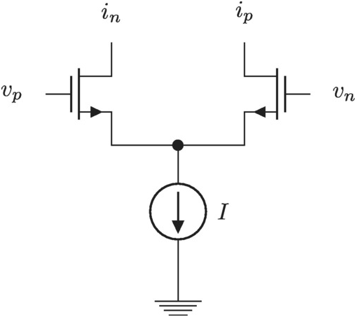
Figure 2.8 Differential pair without degeneration.
Simplify
We will simplify the analysis by assuming all signals are antisymmetric around the center point. This point will become what is known as a virtual ground. Its voltage is constant and is in the AC sense a ground: see Figure 2.9. With this simplification we have
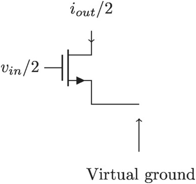
Figure 2.9 Symmetrized differential pair.
Solve
We immediately recognize this as a CS stage we just investigated in the previous section. The only difference is that the input voltage is half of the input voltage to the full two transistor circuit. The output differential trans conductance is now trivially:

which is again identical to our CS-stage analysis, ignoring the input capacitance and source impedance.
Evaluate
We have seen that by utilizing symmetry one can greatly simplify the circuit analysis.
Nonlinear Extension
For a differential pair there is an interesting subtlety concerning the third harmonic. Consider this model of a differential pair where each leg has a drain current
 (2.5)
(2.5)If we approximate the current sink at the source node with an ideal current sink and ignore any degeneration resistor, the sum of the signal currents in both legs needs to be zero.

Where we have assumed vs2≪vg2 . We then have

For vg~ sin ωtvg∼sinωt, we find the source voltage contains the second harmonic of the input signal, vg.vg. This is also easy to convince oneself of with the intuitive idea the source voltage ‘sees’ a pull-up/down from each leg and it occurs at twice the frequency. We have established the common source point sees a second harmonic. This is a well-known result for differential pair operations. Let us know look specifically at the second-order term in the expression for idid equation (2.5), while assuming vg = A sin ωtvg=Asinωt

The last term contains the third harmonic! It is being mixed up by the second-order expansion coefficient. This third harmonic can be significantly larger than the one resulting directly from the third order expansion coefficient. It is an interesting artifact of the differential pair operation. Be aware the inherent limitation in this analysis in that we assume there are no circuit elements with memory, like caps and inductors present so a Taylor expansion applies.
Current Mirror
Imagine now another extraordinarily common topology, the current mirror in Figure 2.10.
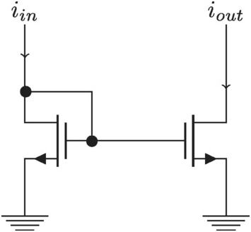
Figure 2.10 Current mirror.
The gain is straight forward and we leave it to the reader to analyze. We will look at the noise transfer of this circuitry. We assume the reader is familiar with the concept of noise and has studied various modeling methods in other courses. For details on our noise modeling see Appendix A.
Simplify
We simplify the circuitry by ignoring any capacitance and assuming there are two noise sources from drain to source for each transistor, as in Figure 2.11.
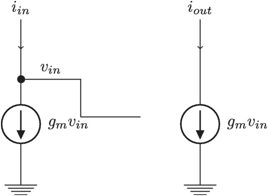
Figure 2.11 Linearized current mirror.
Solve
The noise transfer for transistor M1 is now simply
From the other transistor we now find trivially
The two noise sources are uncorrelated so their power will add. We find
Using the common assumption that in = 4kTγgmin=4kTγgm we have
Later we will look at the output impedance for this configuration and how it can be improved. We will therefore quickly realize the output impedance is
Evaluate
The key lesson here we will use in later calculations is that the noise powers add if they are uncorrelated. Since a common assumption for transistor noise is that its power is ∼gm∼gm we have the resulting noise is proportional to the sum of the transistors gmgm for a simple current mirror configuration.
Simple Cascode Transistor
The output impedance we just studied is often inadequate. A common remedy is to add another CG stage at the output of the current mirror transistor.
Let us look at Figure 2.12 and investigate the output impedance
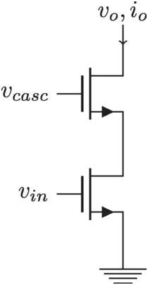
Figure 2.12 Simple cascode transistor stage.
Simplify
We do the same simplifications as earlier and linearize around the bias point: Figure 2.13.
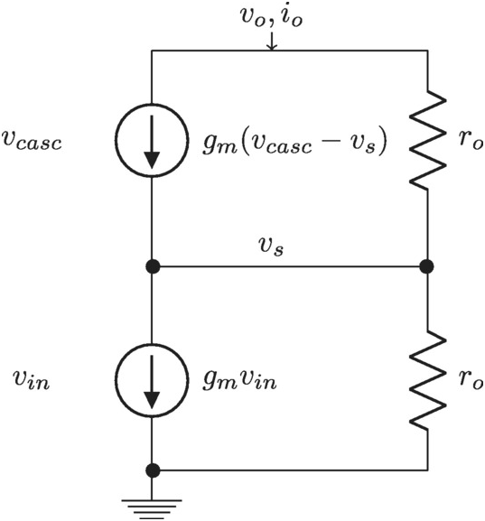
Figure 2.13 Linearized cascode transistor stage.
We also assume the transistors are such the output resistance roro is the same for both transistors.
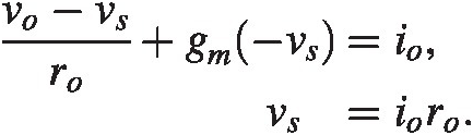
Solve
We know that without the cascode transistor the output impedance is given by (2.6) where roro is the output resistance of a single transistor. With the cascode we find by injecting a current at the output terminal and setting up KCL
Combining we find
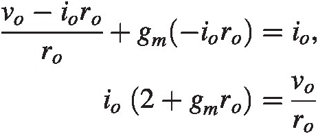
Finally
Evaluate
The output impedance has been amplified by (2 + gmro)2+gmro. In the next chapter we will see another way of boosting the output impedance even further. We will see an example later on in this chapter where the cascode is made up of a thin oxide transistor which can be made much smaller in area than the bottom transistor for a given current, resulting in a reduced capacitive load. This type of cascoding is a very common arrangement to improve isolation and impedance.
CMOS Inverter
The CMOS inverter is another classic, see Figure 2.14.
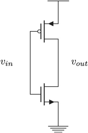
Figure 2.14 A CMOS inverter stage.
This circuit is usually studied with propagation delay in mind [4, 5]. We will study its input impedance over frequency and its gain around the trip point in this section. In the next section we will see how a cross-coupled inverter operates around the trip point.
Simplify
We simplify by looking at the gain around the trip point where the output is equal to the input and we will use the following simplified model shown in Figure 2.15.
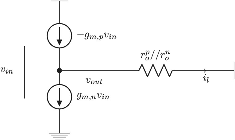
Figure 2.15 A simplified CMOS inverter around the trip point.
The bias of the transistors is such that each is in saturation and the channel charge does not contribute to the gate-drain capacitance. However, we include such a capacitor here since the fringing capacitance can be a significant portion of the overall capacitance for small geometry CMOS technologies. We can now calculate gain and input impedance:
Solve
Let us first look at the DC gain, by ignoring all capacitors. We find
And
 (2.8)
(2.8)Where we have assumed gmgm is the average trans conductance of the NMOS and PMOS transistors and ro=2rop//rop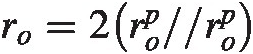 , see [5].
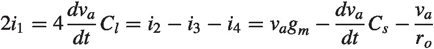
The input impedance at DC is practically infinite (not counting the small leakage current due to tunneling). For the input impedance at some higher frequency we can ignore the shunting capacitor to ground in the first analysis and add it in later. We find now we can use the simple model in Figure 2.16 where we use the average trans-conductance of the two transistors to calculate the gain and impedance. The capacitance for the inverter amplifier is a complicated structure involving even nonlinear entities. Here we will simplify this by assuming the capacitors are constants.
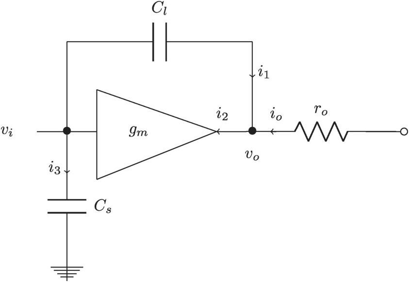
Figure 2.16 Simple model of an inverter where the average transconductance is used.
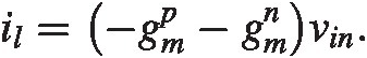
For gain we have from the figure
 (2.11)
 (2.13)
We here use (2.10)–(2.12) to get
and after rearranging:
 (2.14)
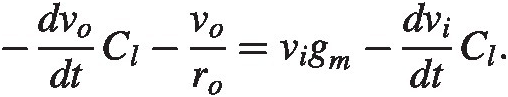
We have this in the time domain at this point since we will use that description later. In frequency space we have
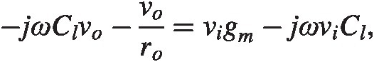
giving
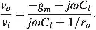 (2.15)
The input impedance can be calculated from
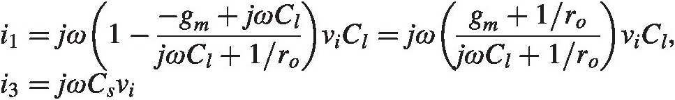
We find
 (2.16)
Verify
This trip point transfer function, (2.15), can be found in for example [5], the rest of the calculations and the derivation of the differential equation can verified either with a simulator or symbolic manipulation software. The dominant time constant is given by ro ⋅ Cro⋅Cl, in line with for example [4]. We also find from (2.15) at low frequencies we recover (2.8). For low frequencies the input impedance (2.16) goes to infinity as we expect, for high frequencies the impedance goes to zero, the shunt capacitance CsCs simply shorts out the amplifier. All this is in line with what one should expect from the model.
Cross-Coupled CMOS Inverter
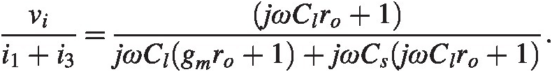
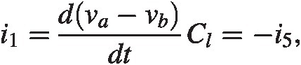
We have taken a quick look at the basic CMOS inverter stage. We will now use what we learned to study a somewhat more complicated system; the cross-coupled inverter. We include here both the input/output shunting capacitor and the input capacitor to ground.
Simplify
We have the following simple description shown in Figure 2.17:
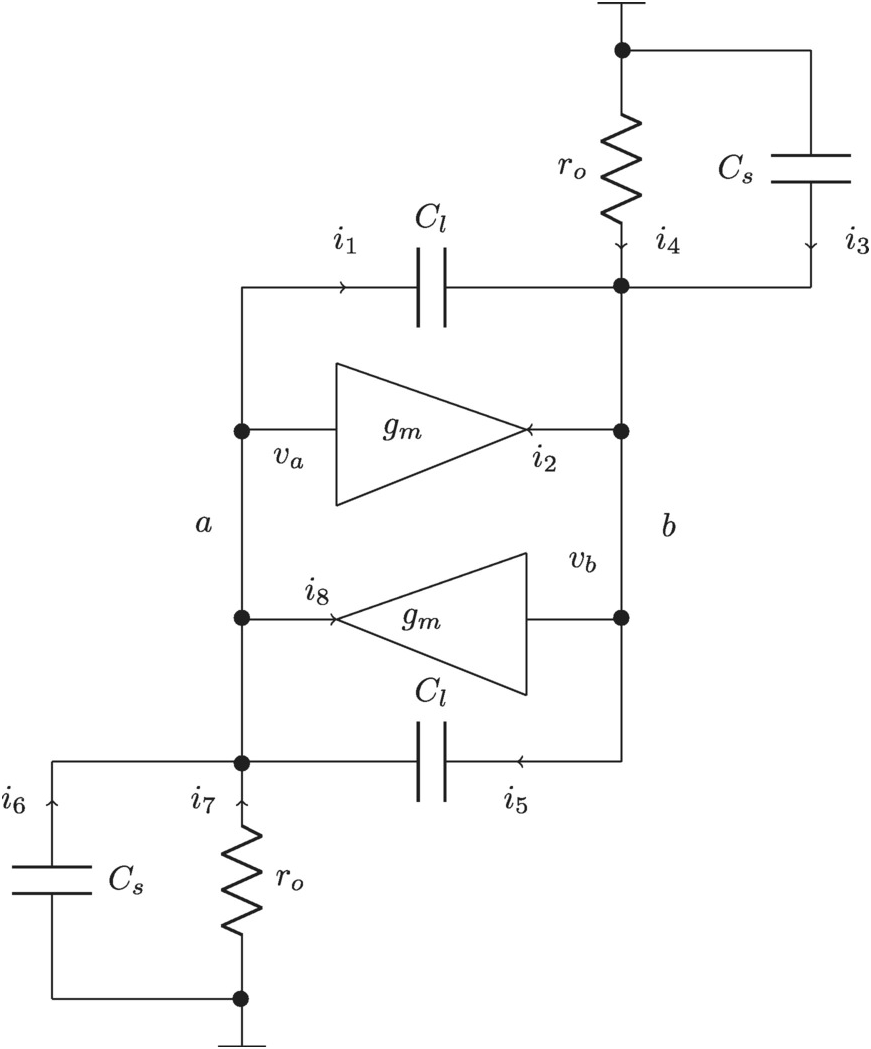
Figure 2.17 Cross-coupled inverter and its simplified model with an input/output shunting capacitor and a capacitor to ground.
This simplification starts to break down when the inverters become unbalanced but as an initial study of such circuits behavior it will prove quite insightful and we will use it in Chapter 3.
Solve
We will first setup the basic loop equations with the labels in the figure.
 (2.19)
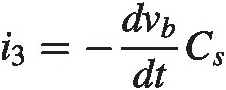 (2.24)
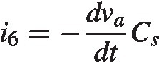 (2.25)
We have 10 unknowns and 10 equations so we should be able to make some progress here. First we see there is an antisymmetry in the problem in that
We find now
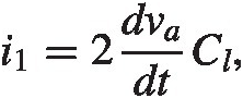 (2.28)
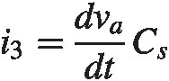 (2.30)
we see by combining (2.26)–(2.30)
A simple rewrite now shows
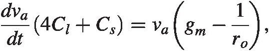
which has the solution
where
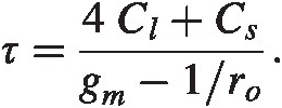 (2.32)
Notice the factor of 4. It results from the simple loop and is akin to the Miller effect. The shunt capacitance, ClCl corresponds to the gate drain capacitance, CgdCgd and CsCs is the gate souce capacitance CgsCgs. In saturation we know from elementary text books Cgs ≈ 2/3 CoxCgs≈2/3Cox. If we look at the fringe gate-drain capacitance in the appendix we see it is about 1/2 of the gate-source capacitance. The total capacitance in the numerator of equation (2.32) is then
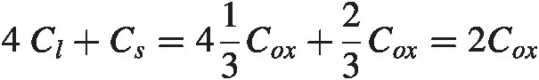 (2.33)
Finally the timescale for our process and using the transistor in Appendix A is
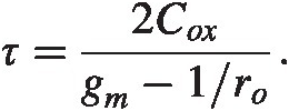 (2.34)
Verify
This can be easily verified in a simulator.
Evaluate
For small geometry CMOS the fringe capacitance gate-drain cannot be ignored. In fact its effect is also amplified by a Miller like phenomenon in cross-coupled pairs. Of interest here is the fact the timescale is not set by ro ⋅ Cro⋅C like we had earlier, the gain of one of the stages rogmrogm speeds up the loop and we are left with a much shorter timescale.
Design Examples
Example 2.3 Current mirror with cascode and large output impedance
In design Example 2.2 we defined the needed output impedance of the current sink for the follower (CD) stage we designed. Let us here design a current sink that can sink the needed current and at the same time provide the required output impedance: for specification see Table 2.3.
Table 2.3 Specification table for current mirror with cascode
| Specification | Value | Comment |
|---|---|---|
| Voltage compliance | >500 mV | |
| Output resistance | >1000 ohm | |
| DC current | 10 mA |
Solution
We know from this technology that a minimum size device has gmro ≈ 10gmro≈10, see Appendix A. With a simple cascode the mirror transistor can then have an output impedance that is 10 times larger than the mirror output impedance by itself. We see from the appendix that a thick oxide transistor with l = 200 nm might suffice: it has an output resistance of about 2.5 kohm. It needs at least 300 mV to be in saturation, Figure A.4. The cascode transistor is then left with 200 mV drain source voltage and from Figure A.2 it seems this is adequate if the gate-source voltage is ~470 mV. The total sink current is 10 mA and this means we can bias a transistor at Vgs~770 mVVg∼770mV and m = 20m=20 instances to get the required current draw for an output resistance of 125 ohm.
We find as a starting point the parameters in Table 2.4:
Table 2.4 Starting point sizes for current sink
| Device | Size | Comment |
|---|---|---|
| M1, thin oxide | W/L = 200 μm/30 n | |
| M2, thick oxide | W/L = 200 μm/200 n | |
| Output resistance | 1.25 kohm | Vout = 500 mVVout=500mV |
The simulator output is shown in Table 2.5. The output resistance is 1.1 kohm at 500 mV which is slightly above our specification. The cascode transistor does not have a gmrogmro that is quite 10, hence the difference from our estimate.
Table 2.5 Final sizing table after simulation optimization
| Device | Size | Comment |
|---|---|---|
| M1, thin oxide | W/L = 200 μm/30 n | |
| M2, thick oxide | W/L = 200 μm/200 n | |
| Output resistance | 1.1 kohm | Vout = 500 mVVout=500mV |
With this current sink design we have together with Example 2.2, a full CD stage we can use in Chapter 7.
2.4 Summary
We have looked at the common transistor gain stages from an estimation analysis angle. We found by stripping away minor contributors to gain and impedance we end up with a simple model of the performance that can be used as a starting point for simulator fine tuning. We also took a brief look at nonlinear extensions to the basic gain-transfer function and we found we can model the effect within a few fractions of a dB over a wide range of load resistance for a particular configuration. The idea can be summarized as one of simplify, solve, verify, evaluate and we showed a handful of examples where this procedure was followed. The purpose was to show the reader the procedure in a familiar territory and we will venture out into less common areas in the following chapters.
2.5 Exercises
1. Investigate common mode properties, gain and output impedance, of the differential pair. Verify!
2. Calculate third-order correction to the CD stage. Verify with the following
vo=−gmRl1+gmRvin+−gm′Rl1+gmR3vin2+2gm′2RlR−gm″Rl1+gmR1+gmR5vin3.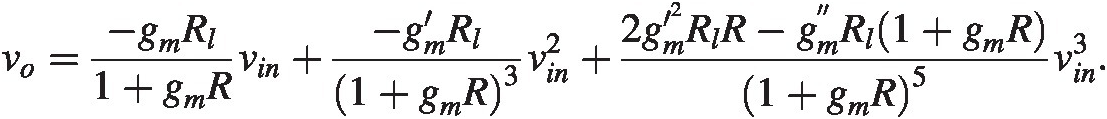
3. Calculate the gain and input impedance of the CS stage where the transistor has a source degeneration impedance. Verify!
a. Derive the second-order correction to the CS stage with a degeneration resistor at the source. Hint, compare with CD stage.
b. Include the nonlinearity of roro.
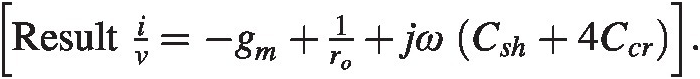
5. In the cross-coupled inverter model calculate the differential admittance by injecting a current between the nodes a, ba,b in Figure 2.17 and calculate the resulting voltage across the pair. This expression will be useful in the later chapters. Resultiv=−gm+1ro+jωCsh+4Ccr.
2.6 References
 Findit@CUHK Library | Google Scholar
 Findit@CUHK Library | Google Scholar
 Findit@CUHK Library | Google Scholar
 Findit@CUHK Library | Google Scholar
 Findit@CUHK Library | Google Scholar