Abstract
The estimation analysis method is described in the context of sophisticated amplifiers. The purpose is to convince the reader of the usefulness of the technique by whetting their appetite with more complex systems. We start with a simple five transistor circuit and move on to comparators and cascaded amplifiers. All these are studied by applying simplifying assumptions followed by analytical solutions. Noise analysis and appropriate scaling techniques are also described in detail. The chapter further contains design examples and exercises to familiarize the reader more deeply with the methodology.
3.1 Introduction
We will discuss somewhat more complex amplifier configurations in this chapter. Following the treatment in Chapter 2 we will here analyze the amplifiers following the estimation analysis method. The calculations will be very similar to the standard literature in, for example, [1–3] and they serve more to showcase the methodology in a familiar setting than to demonstrate any new insights.
We start with the well-known five transistor amplifier, a classic interview question, and continue with cascode stage amplification using feedback. This is followed by a comparator discussion where we put the emphasis on simple timescales and noise analysis. After that, we investigate cascaded stages and the implication in terms of gain, noise, and linearity. Finally we show a couple of design examples that will be used in later chapters where several full-blown design examples will be built and the building blocks we have developed with simple models will be of help in designing the final circuits.
3.2 Five Transistor Amplifier
The classic five transistor amplifier is shown in Figure 3.1. It is used all over the circuit world in all manners of applications. We will here focus on noise transfer but we start with a quick description of its operation.
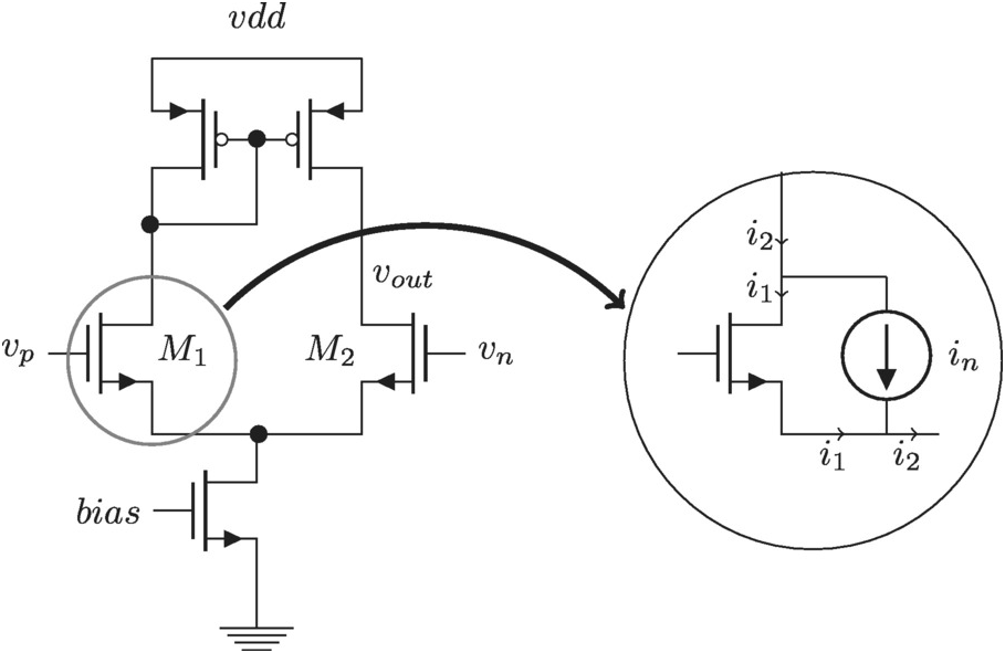
Figure 3.1 Five transistor operational amplifier.
Simplify
First we will simplify by assuming the various transistors have the same combination of gm, rogm,ro. Then we assume the current bias tail transistor has zero output conductance. The amplifier output resistance is modelled as a resistor ro = ro, p//ro, nro=ro,p//ro,n between the output node and supply.
Solve
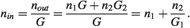
The basic operation of the amplifier is as follows: The transconductance gain of the differential pair is causing a current to go into the load. The load is a simple current mirror and the current from transistor M1M1 is appearing at the output out-of-phase with the corresponding current generated by transistor M2M2. The output voltage swing is finally given by the output current times the load, roro. We find using vin = vp − vnvin=vp−vn
and the gain
Verify
This is a classic calculation that can be found in [3] for example. Let us now look at noise transfer. This is a common interview question.
Simplify
The noise from all the transistors is uncorrelated so the noise powers will add
The noise voltage is small so a linearized version of the circuit suffices to capture the noise transfer function.
The NMOS transistors have the same transconductance, gm, ngm,n and PMOS has gm, pgm,p
Solve
We will solve this by calculating the noise transfer from each of the noise sources and add their power at the output.
Calculating KCL at both the source and the drain shows half the noise current goes through the opposite transistors source node into the PMOS mirror, the other half goes through the same transistor and closes on itself, see the zoomed-in portion of Figure 3.1. The loop formed by the noise current that goes through the opposite transistor causes the current to be mirrored by the PMOS load and the two half currents add up at the output node. We find
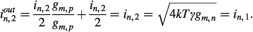
The PMOS current mirroring is much simpler, we have from the section “Current Mirror” in Chapter 2 ipout2=2⋅4kTγgm,p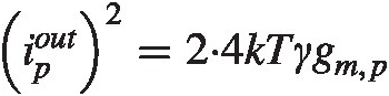 .
.
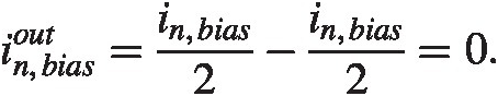
Finally, the current bias transistors current splits into two where one half goes through the PMOS mirrors the other directly to the output load resistor. Keeping track of the sign of the current we find
The total output noise voltage now becomes

And input-referred,
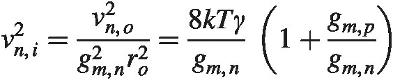
where we have assumed the correction factor γγ, is the same for both NMOS/PMOS.
Evaluate
The final expression here looks deceptively simple. The key realization here is the noise currents for the differential pair transistors actually splits evenly and gets transferred to the output through two different paths.
3.3 Cascode Stage Amplification Using Active Feedback
In Chapter 2 we saw how a cascode transistor improved the output impedance of a current mirror. We can go one step further and we will now show an even higher impedance can be achieved with active feedback. Let us look at Figure 3.2. The amplifier senses the cascode source voltage and amplifies it to drive the gate of the cascode transistor. We will next analyze this within the estimation analysis framework we have been using.
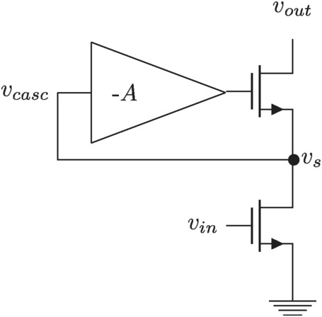
Figure 3.2 Cascode stage with an amplifier in feedback.
Simplify
Let us simplify by assuming the gain has infinite bandwidth. We leave to the reader to solve the finite bandwidth case.
Solve
Similarly to the previous example we have

The only difference to before is the gain A + 1A+1 in front of the transconductance. The result is
Verify
This calculation can be found in [2] for example, where the active cascode case is investigated in detail.
Evaluate
As with the previous example we see a great additional impedance boost can be achieved with a cascode transistor, this time using an additional amplifier in a loop configuration.
3.4 Comparator Circuit
A comparator circuit is shown in Figure 3.3. This so-called strong-arm comparator is a work horse in modern integrated circuit data converters. It has gained this popularity due to its low-power, a few mW is not unusual, high gain and speed. We will analyze the circuit in a few steps where we will employ the estimation analysis to each. It is expected that with such a popular circuit topology there is plenty of analysis in the literature, see [5, 6], to just mention a few and we will intentionally be somewhat brief in our discussion here.
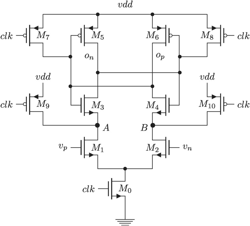
Figure 3.3 Strong-arm comparator circuit.
Comparator Analysis
The analysis can be naturally simplified by dividing it into three phases the circuit goes through as a function of time:
Reset phase. Here transistors M7 – M10M7–M10, turns on pulling the nodes, opop, onon, AA, BB to vdd. Also the switch, M0M0, at the tail turns off the differential pair so the rest of the nodes can be pulled high to vdd.
Initialization phase. The reset voltage goes high enabling the differential pair to be active and releasing the rest of nodes opop, onon, AA and BB. The nodes A, BA,B start to get pulled down by the differential pair until first the NMOS transistors, M3, M4M3,M4 turns on and then the output nodes opop, onon, start to get pulled down until the PMOS transistors M5, M6M5,M6 gate voltage goes below its threshold. The nodes A, BA,B continues down to ground, in effect shorting out the input pair.
Regeneration phase. Here the input pair is disconnected from the circuit operations and the output stage cross-coupled inverters start to decide if the input is high or low.
We will mostly ignore the reset phase here. This is more due to space limitation than to any prejudice against it. We will discuss the last two stages briefly following the steps in the estimation analysis.
Initialization Phase
In the initialization phase the nodes start from their reset voltages, vdd and moves depending on the input voltages more or less quickly to the point where the top PMOS transistors turn on. Here we will first show a possible way to simplify this stage and capture some of its characteristics. We then solve this simplified model and compare to simulations.
Simplify
Let us simplify the operation of this stage by looking at Figure 3.4. We have removed the tail switch and just look at one side of the circuit. We will estimate the timescales to discharge the capacitances at A, oA,o.
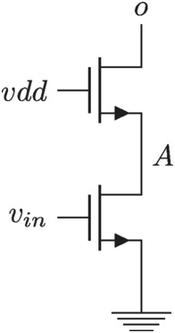
Figure 3.4 Initialization phase of the strong-arm comparator.
Solve
The timescale needed to discharge a capacitance can be found from the governing differential equation, and we will show a simple example here. From basic text books we know that for a capacitor with capacitance CC its charge
where UU is the voltage across the capacitor. Taking the derivative with respect to time gives
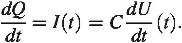
where I(t)It is the current through the capacitor. We can then estimate the timescale, ττ, by approximating dU/dt ≈ ΔU/τdU/dt≈ΔU/τ and find
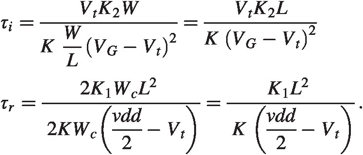
For our circuit we see that node AA gets discharged due to the current going through transistor M1M1. Its capacitance, CACA is set by the combined junction capacitance of M1M1 and M3M3. When the voltage at AA reaches vdd − Vtvdd−Vt, transistor M3M3 turns on. We find
 (3.1)
(3.1)where VtVt is the threshold voltage of transistor M3M3. The current now continues to discharge node AA until it reaches ground and will also discharge the output node, OO, until node OO goes down enough so that the PMOS transistor turns on. Assuming node AA is at ground this results in a timescale for the output node to be discharged of
 (3.2)
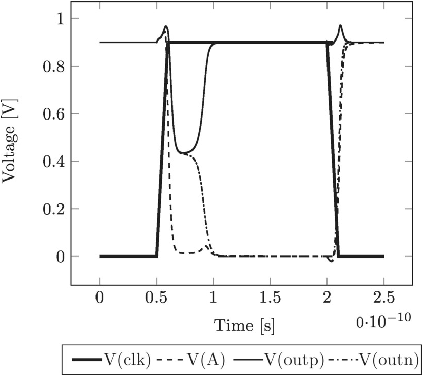
(3.2)where we assume the threshold voltages for transistors M3M3 and M5M5 are the same. In this chapter we will only look at various limits and we will assume the relevant timescale for the initialization phase is either (3.1) or (3.2) depending on the situation. See Figure 3.5a and b for a simulation of the initialization phase, where the input nodes are at the same voltage.
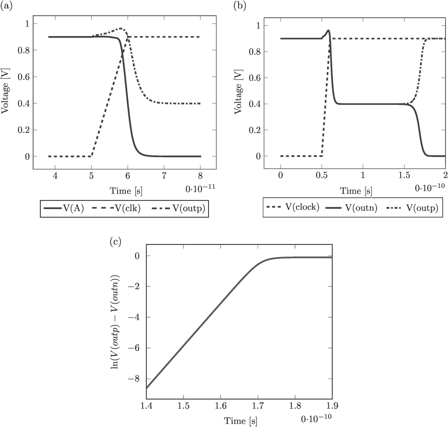
Figure 3.5 Simulation of comparator decision sequence where in (a) and (b) various node voltage are displayed. Figure (c) shows the logarithm of the output differential voltage to indicate the regeneration time scale.
Regeneration Phase
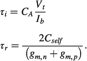
At this stage the transistors start to look like cross-coupled inverters and we will use the results from the discussion in the section “Cross-Coupled CMOS Inverter” in Chapter 2. We know from this section that the time evolution of the system varies like
where
 (3.3)
(3.3)The operation can be easily verified as in Figure 3.5c, where the regeneration cycle can be clearly seen.
Evaluate
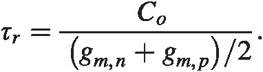
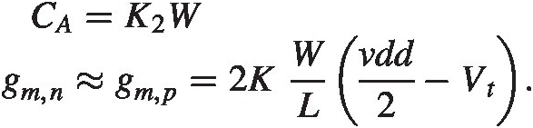
We see from the estimates of timescales that we need to have a large input stage to generate sufficient current and a low capacitive load in order to reduce the time needed to make a decision. With a capacitive load, CloadCload, at the output and the regeneration timescale τrτr from (3.3) shows it is directly dependent on the output capacitance. We need to make sure we have enough transconductance, gmgm in the cross-coupled pair to drive it. With this output load we get using Co = Cload + 2CselfCo=Cload+Cself, where the CselfCself can be found from equation (2.33).
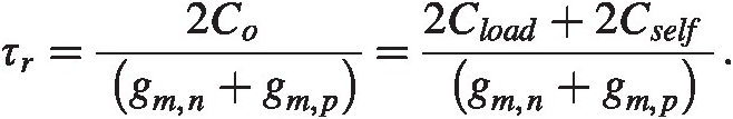
The self-capacitance Cself = 2Cox~WLCself=2Cox∼WL, where we have used the channel width, WW, and length, LL of the cross-coupled transistors. Cload~(W ⋅ L)|loadCload∼W⋅Lload is the load capacitance scaling with its transistor size. We know from elementary textbooks on transistor operation that gm~W/Lgm∼W/L. We then see
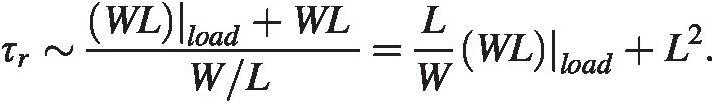
Without the output load we should use minimum length devices for optimal regeneration speed. To minimize the overall timescale the capacitance needs to be minimized leading to minimum width WW of the cross-coupled device. With a specific load we see that a minimum channel length,LL, is beneficial. The width WW should be as large possible to overcome the load capacitance, but will be limited by the capacitance it offers the input stage.
Metastability
The positive feedback nature of the output results in an exponential increase in the output voltage with time
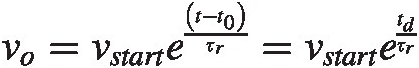
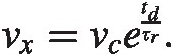
where we have defined the decision time td = t − t0td=t−t0. Imagine now that vstart = 0vstart=0. This would result in vo = 0vo=0 indefinitely. It is called a metastable condition, we will investigate the impact of this phenomenon next with estimation analysis.
Simplify
We will ignore any noise, thermal or other. We will assume there is a certain voltage vxvx that if the crosscoupled pair output exceeds this voltage the following circuitry can operate properly. We will also annotate that given a certain decision time tdtd and regeneration time τrτr, the input voltage needed to reach vxvx in time tdtd is vcvc. We have
We will denote by vFSvFS the full-scale voltage at the input (see Figure 3.6) and finally vLSBvLSB is the least-significant-bit voltage. If the input is within the gray region the output is uncertain.
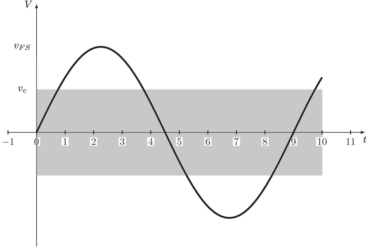
Figure 3.6 Input signal with uncertain decision region indicated in gray.
Solve
Imagine we adjust tdtd or τrτr in such a way as to reduce vcvc by a factor of two. The chance of making wrong decision is now also reduced a factor of two, in that they gray region in Figure 3.6 is half in size. We can then motivate the following formula for the error probability:
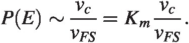
We need to define the constant KmKm and we observe that if vc = 0.5 LSBvc=0.5LSB we will make a wrong decision half the time, or in other words an error rate of ∼100∼100. The constant KmKm needs to be vFS/(0.5vLSB)vFS/0.5vLSB. After some rewrite we have for
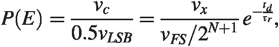 (3.4)
(3.4)where NN is the number of bits in the system.
Input Pair Size
The input pair should be as large as possible while meeting the maximum load requirement at the input. At some point the input pairs own capacitance will dominate its load and further increase in size gives no benefit.
Reset Switch Size
Finally we need to set the reset switches. Fortunately, their operation is relatively straightforward. When the switch is ON it discharges the capacitor in question and the timescale is simply set by the slew rate
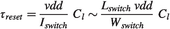
where ClCl is an appropriate load. As with the cross-coupled inverter this transistor also needs to have as short a channel length as possible and as long width as possible. The width will be limited by the load it represents to both the output of the decision circuit and the input transconductor of the comparator.
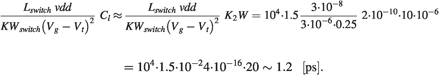
No Output Load
Perhaps a more interesting discussion is the question of how fast one can make this topology for a given technology. Let us look at the various timescales again, but this time we assume there is no load at the output. The input stage still needs to be as large as possible and we will assume its load is dominated by its own capacitance. We have then
For the basic transistor model and parameter relationships, please see Appendix A. We use
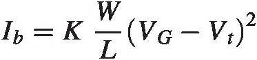
where VG, VtVG,Vt are assumed given. Also
We use for the capacitance at node AA the junction capacitance at its drain
The timescales can now be estimated as
Plugging in the process number for this particular technology from Appendix A, we see
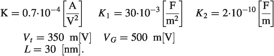
We find
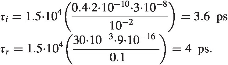
Comparing to the simulator we are in the same ball park τi~3 psτi∼3ps, and τr = 3.6 psτr=3.6ps, which is close to our estimate.
This does not take reset time into account which is roughly
To these estimates we need to add finite clock rise/fall times.
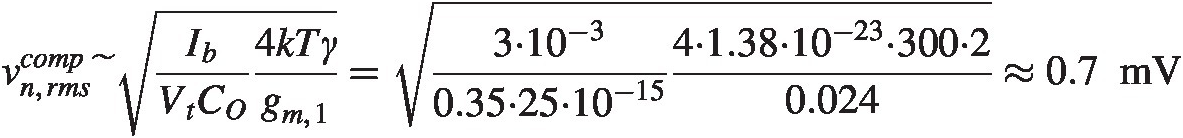
To see where we are qualitywise we can estimate the bit error rate. Let us assume that all timescales are zero except the regeneration timescale τrτr. Let us also assume the sampling rate is 25 GSps or sampling period is 40 ps. Assuming further we have a 6-bit system with a full scale voltage vFS = 800 mVvFS=800mV and a decision voltage vx = 200 mVvx=200mV, we find from (3.4)
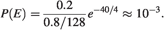
In reality we need to allow some time for the rest of the steps. A typical error rate in communcation systems might be 10−610−6 so we are hard pressed to achieve 25 GSps for these transistors in this technology with a reasonable bit error rate. We can improve the situation by allowing for longer sampling period, using a lower VtVt device or some other such scheme. For instance with a 12.5 GSps sampling frequency we find a minimum bit error rate of
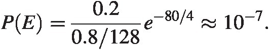
This looks like a better option but recall this would mean we need a duty cycle that is far from 50 percent and the rest of the timescales need to be small.
Comparator Noise Analysis
We will now analyze the noise transfer of the strong-arm comparator following the steps we just used to estimate the fundamental timescales. We will focus specifically on noise transfer and ultimately signal to noise ratio (SNR). We will assume the input signal is sampled already and is constant during the comparator operation. We will also only look for scaling relationships and see how transistor parameters contribute to the noise. This leads to considerably simpler expressions compared with more detailed analysis as found in [5].
Initialization Phase
The noise signal is now assumed to be approximated by the simple noise source across the source-drain of the input-stage transistors.
Simplify
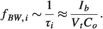
In this stage the clock switch at the bottom of the transconductor is on which activates the input stage. We will assume here that the capacitance of AA is small compared with the full output load, CA ≪ CoCA≪Co, and then the output transistor, M3M3 looks like a CG stage. This is the opposite limit we looked at before when we were interested in maximum speed possible; here we look at the situation where we have an appreciable load at the output. For cases where the input stage is limited in size by the required speed and one uses a typical output load this is a reasonable assumption. We will also assume the input is itself a constant during this phase. Furthermore, we will assume the noise average over the timescales involved is
where we estimate the bandwidth, fBW, ifBW,i, to scale as 1 over a relevant timescale, here
Solve
We will look at this problem in the time domain. The output voltage is simply
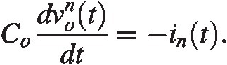
We only know time average noise power∫in2tdt/T=in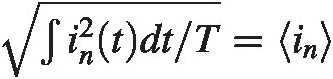 . Therefore the solution to the differential equation can be estimated to be on average
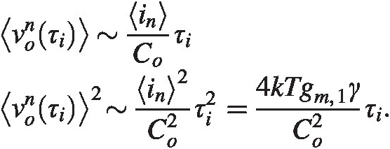
For the signal itself we find similarly, using i(t) = gmvinit=gmvin
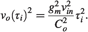
The second transistor does not contribute to noise in this stage with these simplifications.
Regeneration Phase
For the regeneration phase we will again look at Figure 2.17.
Simplify
We now simplify by assuming the drain of the input pair has reached ground so we simply have two cross-coupled inverters. The input transistors are thus disconnected from the output and do not contribute to the noise and not directly to the output during this phase.
Solve
Due to the positive feedback nature of the cross-coupled pair we find again using simple scaling arguments that
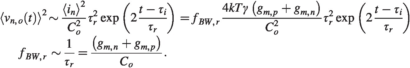
We get

where we have used the timescale from equation (3.2) as the starting point for the exponential growth. The output noise voltage is highly time dependent, and the seed noise at the start of the regeneration phase will grow more than the noise voltage injected at later times.
Final Result
Putting all these together we find the output noise is

The signal at the output is similarly
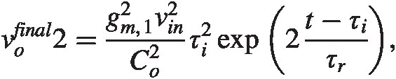
from which we see the gain
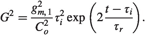
The input-referred noise is now
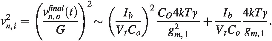 (3.5)
(3.5)Verify
The calculation here is a simplified version of a much more general discussion in, for example, [5], though we get similar information with significantly less effort. However, the full solution in [5] is certainly also valuable.
Evaluate
This means that if we can maximize gm, 1/Ibgm,1/Ib both terms will be small. Bear in mind the initial assumption that the input transistor is limited in size due to bandwidth limitations, which will limit what we can do. A more detailed analysis for the general case where the capacitance at the output of the transconductor is significant leads to similar conclusions.
3.5 Cascaded Amplifier Stages
This section concerns cascaded amplifier stages. In almost any modern electronic system there is more than one amplifier, and combining several together for an aggregate gain and linearity is a key skill. Here too a simplified estimation model can be constructed, as discussed in many books. We include such a model here more for the sake of completeness than in the hope of adding to the reader’s knowledge.
Imagine the situation as in Figure 3.7. We have two amplifier stages where the noise and gain and linearity for both stages are marked in the figure. We will calculate the input-referred noise and linearity.
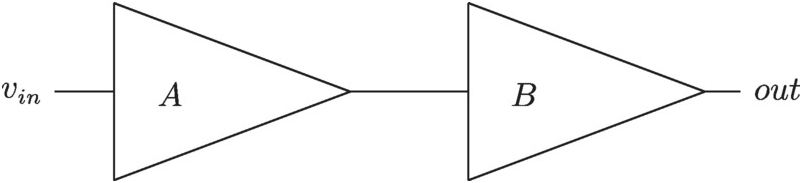
Figure 3.7 Two cascaded amplifiers.
Simplify
We simplify the picture by assuming the noise is not input-dependent and the gain has no phase shift. All entities are in power, as V2/RV2/R.
Solve
Let us first calculate the overall signal gain at the output. This is straightforward.
The noise at the output is now
The input-referred noise is simply this quantity divided by the gain
The total input-referred noise due to n2n2 is reduced compared to n1n1 by the gain of the first stage. Thus a high gain at the input will reduce the impact of noise at the subsequent stages. This is a useful property.
The linearity behaved differently, as we can see from Figure 3.7. At the output

where we have only kept terms up to third order. Divide by GG to get the input-referred power finds
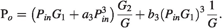
We now see the non-linearity caused by the second stage is amplified by a factor G13/G=G12/G2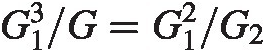 . In this case having a large gain upfront is detrimental to performance.
Evaluate
The important thing to remember here is that for noise optimization it is convenient to have a large gain up front while for linearity optimization the gain should be small in the first stage. This inherent juxtaposition significantly complicates receiver design.
Design Examples
Example 3.1 Comparator Design
We will here discuss a comparator design based on the specifications detailed in Table 3.1. We will use this design in Chapter 7 when we design a full ADC.
Solution
With the timescaling rules discussed in the section “Comparator Analysis” it is fairly straightforward to size up the circuit. With different specifications one might use a different approach. Here we will
1. Size the input stage to be as large as maximum load specification allows. We know from the scaling rules we need the input stage to be as large as possible.
2. Size the cross-coupled pair to be large enough to meet the regeneration timescale specified.
3. Size the reset switches to be large enough to reset the nodes in roughly the initialization timescale.
The input stage should be three-unit transistors from Appendix A to meet the input load requirement. This will provide about 18 fF input capacitance, which is close to what is needed. From this size we know the output junction capacitance is about 6 fF. The cross-coupled pair should then be sized so that they are as large as possible without overly loading the input pair. The initialization timescale is perhaps five to six times shorter than the regeneration timescale, so for sizing concerns the regeneration timescale should be the focus. A cross-coupled transistor pair with nf = 10nf=10 will provide around 2 ∗ 2CoxCox capacitance as a load or around 32 fF with the transistor in Appendix A. We should start with this size of transistor, which will be around 5× the output load of the input pair (6 fF). For estimated and optimized parameters see Table 3.2.
Estimated and simulator optimized sizes for comparator decision circuits
| Device | Size | Comment |
|---|---|---|
| M1, thin oxide | W/L = 30 μm/27 n | |
| M3, thin oxide | W/L = 10 μm/27 n |
Simulator optimization.
| Device | Size | Comment |
|---|---|---|
| M1, thin oxide | W/L = 30 μm/27 n | |
| M3, thin oxide | W/L = 16 μm/27 n |
Our initial estimate of the size is quite close to what we found with the simulator. The reset switches are finally sized so the output nodes are reset properly in roughly the initialization timescale. We find the final sizing in Table 3.3:
Table 3.3 Final size for comparator circuit including reset switches
| Device | Size | Comment |
|---|---|---|
| M1, thin oxide | W/L = 30 μm/27 n | |
| M3, thin oxide | W/L = 16 μm/27 n | |
| Mreset, thin oxide | W/L = 16 μm/27 n |
Figure 3.8 shows a simulation of the final sizing of the comparator.
Noise Estimation
The noise can be estimated from equation (3.5)
Example 3.2 Amplifier with follower
This section discusses a common amplifier design with a low impedance output buffer. It will be used in Chapter 7 as part of a larger ADC design. The specifications in Table 3.4 is a result of a system evaluation of such an ADC.
Table 3.4 Specification table for amplifier with buffer
| Specification | Value | Comment |
|---|---|---|
| Input capacitance | <10 fF | Driven by 10 ohm resistor but with 64 amplifiers in series, providing a time constant of 10 fF ∗ 10 ∗ 640 = 6 ps |
| Gain | >2 | From system |
| Output load | 20 fF | Differential input stage |
| Output impedance | ≪100 ohms | From system |
| Output common mode | 650 mV | From system |
Solution
Given the low output impedance and the low input capacitance it seems best to work with the topology shown in Figure 3.9.
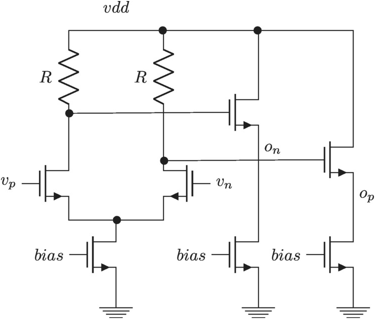
Figure 3.9 Amplifier with output buffer.
The sizing is relatively straightforward. We will use the transistor size from Appendix A, which gives m = 1m=1. The load will be set by the gain to be around 300 ohm, with a gm = 8 mmhogm=8mmho for the transconductor that will provide a gain of about 2.5. The bias current will be set by 2 mA from the bias of the unit transistor and the output follower will also be a unit size transistor since that has an output impedance of about 10 ohms. In summary the parameters will be as in Table 3.5.
Table 3.5 Starting point which is also final sizes for amplifier
| Device/Parameter | Value | Comment |
|---|---|---|
| M1, M2, M3, M4, channel width/length/nf | 1 µm/30 nm/10 | |
| Load resistor | 300 ohm | |
| Input current | 500 µA | Leaves a gain of 4 for main bias |
| M4 channel width/length/nf | 2 μm/250 n/10 | Thick oxide device |
| M5 channel width/length/nf | 2 μm/250 n/40 | Thick oxide device |
| M6 channel width/length/nf | 2 μm/250 n/20 | Thick oxide device |
| Supply voltage | 1.4 V | To get the output common mode correct |
For this case all the relevant properties have already been characterized and one would expect the simulation to line up closely to the estimated numbers. One thing to note is that the load resistance is about a third of the transistor output impedance. One cannot make it much larger and expect the corresponding benefit of gain increase.
3.6 Summary
We have looked at more complex transistor gain stages from an estimation analysis angle. We used the time description of the circuit equations when discussing comparators and we used several single pole analyses to get a handle on the timescales and noise transfer in a strong-arm type of comparator. We found that fairly simple arguments can be used to come close to solutions that are based on more detailed models. It is another example of the applicability of estimation analysis where we consider the core behavior of the system and try to capture it with simple modeling. The steps simplify, solve, verify and evaluate were used time and time again and we used the transistor size parameters suggested by simple modeling as a starting point for the simulator fine-tuning. Finally we looked at cascaded amplifier stages where well-known relationships between noise and linearity were derived following the estimation analysis steps.
3.7 Exercises
1. Redo the noise analysis for the five transistor circuit where the bias transistor is replaced by a bias resistor. Do not rush into the calculations. Instead, simplify and estimate.
2. Redo the comparator noise analysis where the capacitance at the drain of the input pair cannot be neglected. Simplify, Solve, Verify, Evaluate!
3. Improve the cascaded feedback amplifier model by assuming the amplifier has a finite bandwidth. (Treat it as a single pole at ω3 dBω3dB.)
3.8 References
 Findit@CUHK Library | Google Scholar
 Findit@CUHK Library | Google Scholar
 Findit@CUHK Library | Google Scholar
 Findit@CUHK Library | Google Scholar
 Findit@CUHK Library | Google Scholar
 Findit@CUHK Library | Google Scholar
 Findit@CUHK Library | Google Scholar
 Findit@CUHK Library | Google Scholar
 Findit@CUHK Library | Google Scholar