Abstract
The observations from the is applied specifically to integrated circuit situations, where transmission line effects, inductors, capacitors and S-parameters are discussed using the estimation analysis method. Many useful formulae are derived that are used to design real world inductors and estimated parasitic capacitances. Also a brief overview of the connection between the printed circuit board and on-die applications is presented as well as a summary of the current state of detailed modeling of interconnect effects. The theoretical underpinnings behind common shielding techniques is discussed using the estimation analysis in the last part of the chapter. It is followed by design examples and exercises.
5.1 Introduction
This chapter discusses applications of electromagnetism mainly in the context of integrated circuits with the help of estimation analysis. The main purpose of this chapter, as with the other chapters, is to showcase estimation analysis. We will think of ways to simplify a problem, verify that we capture the relevant properties, and then evaluate the result. At the end of the chapter we will use these simplified models in several design examples to establish a starting point for fine-tuning in simulators.
In recent decades, high frequency electromagnetic effects have become increasingly important for on-chip circuit design with the increase in speed and required processing power. Compared with general microwave situations, the length scales under consideration are smaller than typical wavelengths and this provides some natural simplifications for the estimation analyses. Since we are also approaching speeds where the wavelength is comparable to the circuit size scales, we will discuss short wavelength effects in this chapter. Much of what we will be discussing has been touched upon, one way or another, in references [1–18].
We start the chapter with a discussion of the connection between printed circuit board designs and on-die designs. Thereafter we discuss transmission lines and distributed effects. The concept of S-parameters can often be confusing, and we take some time to discuss it from an estimation analysis perspective. This is followed by a section on capacitors, and since this is generally well known, we will be somewhat brief in this discussion. Traditionally they were designed as overlapping metal plates, but with the advance of small geometry CMOS this topology is no longer used much. Instead, MOM (metal–oxide–metal) capacitors where thin, inter-digitized fingers provide the desired capacitance are used. The advancement in lithography has made it possible in modern CMOS technologies to produce such capacitors with much smaller process variation than earlier varieties, and we will briefly discuss the circuit implications. Of course, gate-over-oxide constructions are another approach, and we address this in the section on metal plates. Thereafter we discuss on-chip inductors, where we model various idealized situations and, by removing these idealizations, come to a realistic model of on-chip inductors where capacitance and resistance are also major contributors.
5.2 Connection to PCB Designs
Printed circuit board (PCB) designers have encountered high speed, or distributed, effects for many years not only through fast clock frequencies but also through fast edge rates, and it is only recently that on-die circuit designers have been forced to take such effects into account. On die, the convenient long wavelength approximation was for a long time sufficient for the interconnect modeling. Normally, distributed effects became important in the package interface. Nowadays, these effects have creeped into the on-die interconnects due to the ever increasing need for higher and higher speeds, and a thorough understanding of these kinds of effects has become mandatory. A good description of the problems can be found in [7]. Here many of the electromagnetic properties we found in Chapter 4 are discussed more fully in connection to the PCB design. We will mention just a few of the similarities here and point to what is different, and where different approaches may sometimes be necessary.
Interconnect Scale vs Wavelength
Distributed effects start to become prominent when the wavelength in question, λ = c/fλ=c/f where cc is the (local) speed of light and ff the signal frequency, is similar to the physical length. The important comparison scale turns out to be even smaller than λλ and we will derive such results in this chapter. Imagine we have a 10 GHz signal traveling in a uniform medium with a permittivity of 4, we find λ = 1.5 ⋅ 108/1010 = 1.5 cmλ=1.5⋅108/1010=1.5cm. On a printed circuit board this is a very small distance. On die, this is fairly large. Ten GHz used to be a respectable frequency, but now imagine a 50 GHz signal. The wave length is 3 mm. A modern high speed integrated circuit can easily be a centimeter or two per side, of which the analog portion is significant. It is then clear that issues such as proper termination to avoid reflections is important.
Ground Planes
These distributed effects were understood very early on in the development of the circuit board, and the concept of proper ground was developed. A modern circuit board can have many tens of layers of copper, each of which is perhaps 15 µm thick, and every second layer is typically used either as a ground or supply plane. On die there can also be more than ten layers, but in contrast to the circuit board system the thickness is only significant (greater than the skin depth) for a few of the top layers. Using lower metals for the ground/return path is woefully inadequate. Instead, co-planar wave guides or multilayer ground planes are commonly used.
Vias
A circuit board via consists of a top/bottom pad and a thin metal cylinder. The pad looks capacitive and the thin cylinder looks inductive, and it can also exhibit distributed effects. An on-die via is simply a stud, often made of tungsten, and its resistance can be significant. One needs to make sure there are plenty of vias when significant current is in play.
Summary
As a short summary of similarities and differences between PCB work and on-chip design, we have:
Similarities:
Length scale vs wavelength
Need for proper termination
Differences:
Thickness of metal layers
Resistance of vias
5.3 Recent Progress in the Literature on Signal Integrity On-Chip
Over the last several decades there has been a continual need for increased communication speed. Looking at the state of the art a few decades ago, it was not obvious that on-chip inductors would ever be prominent. But the work of the design group under Prof. Robert Meyer at University of California at Berkeley made clear that on-chip inductors have significant advantages. With the ever smaller footprint, the size of inductors can sometimes be prohibitive, but the increase in required speed and thus smaller needed inductances make inductors a key component in high speed designs, where low phase noise oscillators are obvious circuit applications. At speeds in the 100s of GHz range, the problematic passive device is no longer the inductor, which is now very small, but rather the parasitic resistance of capacitors that causes degradation.
This “need for speed” has generated faster and faster integrated circuits, and we are now at the point where the circuit size is of the same order as the wavelength of the signal frequency we are trying to process. The interest in careful modeling of interconnects has likewise increased and several approaches have emerged. For one, accurate and fast simulators that can handle this size and frequency are constantly being developed and improved. Many of the modern simulators have user-friendly interfaces that facilitate setup and simulation. A word of warning to the user, however: oftentimes there are assumptions more or less hidden inside these simulators that may or may not be helpful in solving the problem one is addressing, and one would be wise to spend a good deal of time understanding the inner workings of the tool before embarking on large simulations. Second, the need for accurate analytical understanding has increased in lockstep with simulator developments. Researchers have developed complex models, and we will present an overview of this development in the next section where the focus is on inductor modeling; see also [19] for a recent overview of the field.
Inductor/Interconnect Modeling
Inductors have a high impact on high frequency performance and their modeling is critical to the success of such circuits. One difficulty with inductor modeling is it can take a bit of time to find the right size combination through field solver iterations. In fact, this is one reason that a good initial size estimate, which we will describe later in this chapter, is important. In the literature, the search for accurate inductor modeling is proceeding along several lines of inquiry. One possibility is to use foundry-supplied inductor libraries (see [20–22]), which tends to limit the ability to use an optimal size, but if one finds a reasonable candidate one has access to measured data, which is reassuring from a performance perspective. Another trend is to create various detailed analytical models as in [23–26], ππ-models as in [27–30], or 2 ‐ π2‐π models as in [31] to predict inductor performance. There is also [32], where regularization theory is applied to obtain more detailed analytical mapping functions. Another direction was proposed by [33], where machine learning techniques are used to build inductor models. The accuracy is improved by only optimizing promising inductor candidates in EM-solvers instead of simulating each possible inductor, as in [34]. Another approach uses a set of EM-simulated inductors as the design space and the optimal inductor is chosen based on various constraints, as in [35, 36]. The arrival of 3D integrated circuit topologies has generated much work relating to through-silicon-vias (TSV), as in [37–40]. These topologies are there to process data faster in that with the help of TSVs, more data can be transferred vertically, which means a much shorter physical distance and less signal loss is possible.
We have highlighted a handful of situations where several groups have attempted to construct detailed models.
In this chapter we will apply the lessons from Chapter 4 to build useful simple models where the physics of, say, an inductor play a central role. It turns out that having the intuition built from such models is very useful in understanding real situations and can generate a good initial starting point for field solvers.
5.4 Transmission Line Theory
Basic Theory
The focus in this chapter is integrated circuit applications, and here, in general, transmission line effects are not important due to the small length scales involved. However, there are instances, for example inductors, where basic knowledge of transmission line theory is important. We will therefore discuss the basic theory here using estimation analysis, and we refer the reader to the many excellent discussions of the full theory in [2, 5–7, 13].
Simplify
A transmission line has essentially two components, one signal conductor and at least one return path as in Figure 5.1.
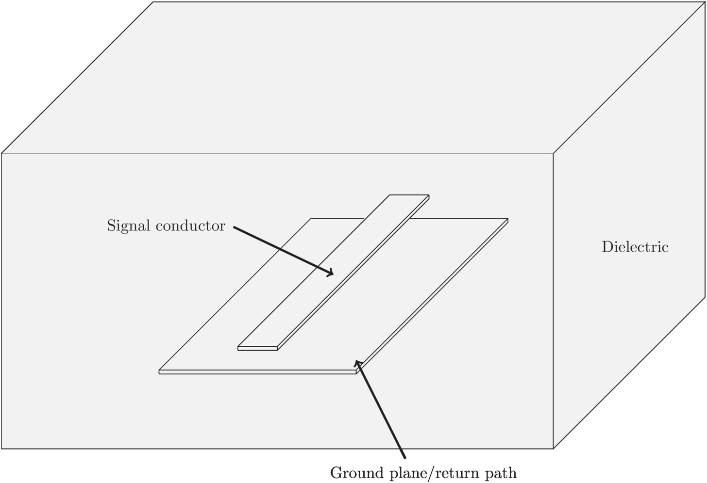
Figure 5.1 Transmission line components.
As we discussed in Chapter 4, this type of structure carries a certain inductance and resistance per length and a certain capacitance to ground per length. In addition, there is a loss in the dielectric medium that we will ignore here. We will model this as a simple RLC filter, as in Figure 5.2. We ignore any loss in the dielectric medium itself, often modeled as a shunt resistor to ground. We are interested in estimating effects such as gain and impedance on-chip, and for common materials inside integrated circuits this loss is negligible.
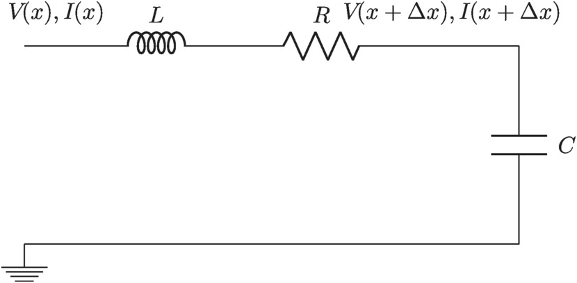
Figure 5.2 Basic transmission line modeling.
Solve
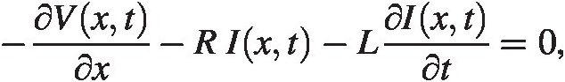
We can now analyze the voltages and currents using Kirchoff’s current/voltage laws:

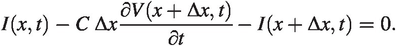
By dividing by ΔxΔx and go to the limit Δx → 0Δx→0 we find
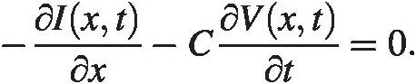
We now use the assumption we are in a steady-state condition where the time variation scales as ejωtejωt. The equations then look like
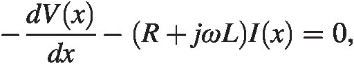 (5.1)
(5.1)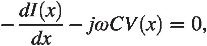 (5.2)
(5.2)Now taking the derivative with respect to x and combining the two we find


The constant in front of the current and voltage terms is known as the propagation constant, γ=R+jωLjωC . The solution is well known


Where the + refers to a wave going in the positive x-direction and the – refers to a wave going in the negative x-direction. We can use (5.1) above to write the current as

We now see we can identify a characteristic impedance as
 (5.3)
(5.3)We find

Let us now terminate the transmission line with a load ZLZL at x = 0x=0. We then can define an impedance as a function of x as

At x = 0x=0 we get

We now find

Γ is known as the reflection coefficient. We can now write
 (5.4)
(5.4)For R = 0R=0 this simplifies to
 (5.5)
(5.5)Where we have complied with the norm in the literature and refer to xx as –x–x. Let us now look at the special case where ZL = 0ZL=0 and R = 0R=0. We have Z0=L/C
 (5.6)
(5.6)which approaches

We see that when ZL ≪ Z0ZL≪Z0 the transmission line looks inductive with a total inductance LxLx. We need to keep this fact in mind when we discuss inductors, because we must not terminate an inductor at high impedance. We will come back to these equations.
Naturally, for the opposite case where ZL = ∞ZL=∞ we find

When terminated with an open the transmission line looks like a capacitor.
It is also instructive to see from (5.6) that at

The impedance goes to infinity. Above this length the impedance changes sign and becomes capacitive in the case of an inductor. This is known as a λ/4λ/4 resonance. There are also resonances at odd integer multiples of this length scale as is clear from (5.6).
CAUTION: One of the difficult parts of microwave engineering is the fact there can be many solutions to Maxwell’s equations. For a given boundary there can be many possible modes when the wavelength is similar to the size of the structure. Identifying these modes and removing the unwanted ones is among the major tasks in microwave engineering. For our particular case of a terminated transmission line, sometimes the symmetry or ground plane or other neighboring conductors can cause the electrical length of a λ/4λ/4 resonance to be different from what one would expect from a simple trace length calculation. For instance, a single loop inductor can be seen as a transmission line with its own return path where the halfway point, the termination, is a short. The electrical length will then be half of the physical length of the inductors coil. We will not address the precise root cause of such situations here since it is outside the scope of the book, but we encourage the reader to always verify the resonance location with a simulator. The good news is when the simulator does not agree with a naïve length calculation, it will find a length that is shorter by some integer factor. The resulting resonance frequency is thus higher than one would expect. Here, our calculations will always use the simulated resonance length if it is different from a simple trace calculation.
Verify
This is a standard result that, if not expressly given in the many books discussing this subject, can easily be confirmed. See for example [2, 5–7, 13].
Evaluate
The impedance of a transmission line depends heavily on its characteristic impedance as well as on how it is terminated. This is most clearly seen in the λ/4λ/4 effect, where the load impedance is effectively inverted when looking from the source point. If one terminates the transmission line with a short it will look inductive when the electrical length is short compared with wavelength, and if one terminates with an open the transmission line will look capacitive.
Key Concept
A transmission line terminated at low impedance, say 0 ohms, looks like an inductor when size ≪ wavelength. A high impedance termination causes the line to look like a capacitor when the size ≪ wavelength.
Key Concept
A λ/4λ/4 resonance is a situation where the length of the conductor is one-quarter of the wavelength. This will transform the impedance at the termination inversely.
Summary
We have applied the estimation analysis to the fundamental concept of a transmission line and demonstrated that we can reach the known solutions with simple mathematical manipulations.
5.5 S-Parameters
Scattering parameters or S-parameters are a fundamental tool in microwave engineering. For the electrical circuit engineer they can often be difficult to conceptualize, and we will show that we can define them in circuit theory (long wavelength approximation) where they are easier to understand. From there a short wavelength extension can be made. We again follow the steps of estimation analysis and build a simple model we can solve to demonstrate some fundamental properties.
We will start with the general definition and refer the interested reader to literature for the details behind them. The discussion follows closely what is often referred to as generalized S-parameters or power waves (see [2]), but here we make the additional assumption that the termination resistor is the same both at the source and the sink, and the degradation is modeled as an impedance between these points. We will then look at a simple circuit version of these parameters and show through some examples how they behave and are related to more familiar concepts such as bandwidth. The last section will discuss the short wavelength generalization.
Definition
From the picture S-parameters are defined as the ratio of incoming or outgoing wave amplitudes in different ports (Figure 5.3).

Figure 5.3 Multi-port system showing in-/outgoing waves.
For example, S11 is the ratio of the outgoing wave amplitude to the incoming wave amplitude when all other ports are 50 ohm terminated. S21 is the ratio of outgoing wave amplitude at port 2 divided by the incoming wave amplitude at port 1, all other ports being terminated to 50 ohms. Notice the concept of outgoing and incoming waves: this is a concept with meaning in the short wavelength approximation but it has no natural meaning in the long wavelength limit. Let us keep this in mind in the following discussion.
Simplify
We will now simplify the situation to the circuit world or long wavelength approximation. Let us consider the following simple picture (Figure 5.4).

Figure 5.4 A simple model of an input configuration.
This is a voltage source in series with two resistors. The voltage at point “vout” is clearly vs/2vs/2 at all times. What if we change the load resistor by adding a resistor RR in series (Figure 5.5)?

Figure 5.5 A simple model of an input configuration with an additional series resistor.
Solve
Now the output voltage will be

We can manipulate this in the following way

where we have defined an “incoming” and “outgoing” wave. In this context S11 is simply

We see that if RR is zero, S11 is zero. Let us think of a more complicated situation where the load consists of a cap shunting a 50 ohm resistor (as in Figure 5.6):

Figure 5.6 A simple model of an input configuration with a shunting capacitor.
We find

We see here again we can define S11 and find

For small CC we see S11 is zero, for large CC S11 = 1. What about S11 and bandwidth of the load itself? At bandwidth we have by definition RtωC = 1RtωC=1 and we see for this case

How far from the bandwidth do we need to be to get S11 = −20 dB?

which is ~5 times the bandwidth of the unterminated input! The reader should by now appreciate the difficulty in getting low return loss for a given system.
What about the other S-parameters? Let us look at S21 using the model in Figure 5.7.

Figure 5.7 A simple model of an input configuration with a series source resistor.
Here we look at the termination as ideal RtRt ohms and the driving impedance is different compared with our earlier discussion. We have with a resistive driving impedance

The energy that goes into the output load is simply the outgoing wave.
At the input we see the driving impedance as RtRt ohms with a load that looks nonideal. With a real nonideality we see

We identify again the first terms as the incoming wave and the last term as the returned amplitude.
We can now identify the various S-parameters:
 (5.7)
(5.7)We see now

For this sum to equal one we are missing a term

What happened to it? Since the square of the S-parameters has something to do with power, let us take a step back and think about this situation in terms of power. We have a current

How much power is being burnt in the various resistors?

Let us normalize this to the power burnt in the load termination resistor when R = 0R=0.

We get by normalizing the actual powers in the various resistors to this ideal power,


The last equation shows the missing term from the equation above. It is simply the power burnt in the parasitic resistor RR compared with the power burnt in one termination resistor in an ideal situation. The rest of the terms correspond to the power burnt in the load resistor and the power burnt in the source resistor by the return wave.
Key Concept
When the interconnection is resistive it will burn power, so the sum of the square of S11 and S21 is less than one.
What about the partly inductive interface in Figure 5.8?

Figure 5.8 An inductor in series with the source impedance.
Here

This energy that goes into the output load is simply the outgoing wave.
At the input we see the driving impedance as RtRt ohms with a load that looks nonideal. With an inductive nonideality we see

We identify again the first terms as the incoming wave and the last term as the returned amplitude.
We can now identify the various S-parameters:


We see now

We can also calculate S21 for the system with a shunting capacitor. We find


We can now infer that in a purely reactive environment, the sum of the square of the S-parameters is 1; there is no power lost in the medium. The formal proof is beyond the scope of this book.
Key Concept
If the interconnect is purely reactive, the sum of the square of S11 and S21 is equal to one; there is no power burnt in the interconnection.
For the previous two examples it is obvious that S12 = S21 due to symmetry. But this is in fact generally true for reciprocal systems (no active devices, ferrites, or plasmas) (see [2]).
Finally, we wrap up this section with an example of how to estimate insertion loss (S21) for a resistive transmission line. Imagine the following situation depicted in Figure 5.9:

Figure 5.9 Geometry of a single ended transmission line.
We have a transmission line characterized at high frequencies where the skin depth is smaller than the conductor dimensions. It runs over a perfect ground plane (we will generalize this later to a real ground plane).
Simplify
We know that the current will run in the bottom of the conductor to minimize the magnetic field, and we know the width of the wire and the skin depth. In Figure 5.10 we have, assuming the dielectric extends beyond the conductor strip,

Figure 5.10 A cross-sectional view of the single transmission line.
So

The width of the skin depth in the ground plane is
Where we have approximated the extension beyond the edge with a generalization of our findings in section “Currents Induced in Perfectly Conducting Ground Plane” in Chapter 4. At first, we will ignore the resistance of the ground plane for simplicity. It will be simple to generalize later.
Solve
We now need to calculate the line impedance with the characteristic impedance from (5.3) and a termination impedance ZL = RtZL=Rt. We get from (5.4)

We will first look at this from the small electrical length perspective where γxγx is small.

We now get by using equation (5.3) for

which is a fairly intuitive result.
We see then from equation (5.7) that
 (5.8)
(5.8)Verify
The transmission line was modeled as a fixed length ≪λ/4≪λ/4 to avoid distributed effects in line with our previous modeling assumptions. The excitations were modeled as wave ports. From Figure 5.11 we see field solver shows excellent agreement with our theory up to Rx/Rt ≈ 0.1Rx/Rt≈0.1. After this point there are higher-order effects that start to become important, but we are still within 0.5 dB at Rx/Rt = 0.5Rx/Rt=0.5.

Figure 5.11 A comparison of simulated vs estimation of the loss in a single transmission line.
Evaluate
The S-parameters can be understood from a simple local picture through the use of generalized S-parameters and power (voltage) waves. Depending on the situation, a number simple scaling laws are easy to derive and confirm.
Summary
There are a couple of convenient microwave theorems useful to keep in mind for passive systems. If the passive system has no resistance, we must have

In particular for a two-port system:

something we just exemplified.
Another convenient nugget is for a reciprocal system
and for a two-port system
S-Parameters for Long Transmission Lines
In the previous section we looked at a short transmission line where the length was much less than a wavelength. Here we will discuss the more general case of arbitrary length t-lines and the resulting S-parameters. This section will tie together a few of the things we discussed earlier in the chapter.
We have the following situation depicted in Figure 5.12.

Figure 5.12 Pic of t-line in series with termination resistor.
Simplify
We will assume the resistance per unit length, R ≪ ωLR≪ωL. We then have for

and

where

Solve
We know from (5.4) that the impedance looking into the transmission line from the source port is

Following the S11 discussion earlier, we have the voltage at the t-line input is

where we have defined an “incoming” and an “outgoing” wave. We find

This expression can be found in most textbooks. Plugging in the numbers we now find

Or in terms of magnitude

For S21 we again look at the voltage at the destination port. We have from Section 5.4

where V0+ denotes the outgoing wave into the port and V0−
 the reflected wave from the port. We have

In the limit of small xx we get

We also see that if we keep xx small and vary RR by changing resistivity of the metal, S21 varies with RR like

Evaluate
The S-parameters for a long transmission line can be estimated by looking at the impedance at the input of the line and from there calculating the return loss. The through response can be estimated from the results of wave equation directly.
5.6 Capacitors in Integrated Circuits
Capacitors in integrated circuits are oftentimes well understood by engineers. Here we will discuss them very briefly for the sake of completeness. We start with plate capacitors, which were more commonly used in older technologies, and continue with finger capacitors, which are used with modern CMOS processes.
Capacitors in Integrated Circuits: Plate Capacitors
The MIM cap, or metal–insulator–metal capacitor, is an older type of capacitor. It consists of two large plates with a thin insulator between them as shown in Figure 5.13. In modern CMOS processes they are generally no longer available. The closest approximation to a plate capacitor is the MOS cap, where the top plate is the transistor gate and the bottom plate is the transistor body.

Figure 5.13 Basic capacitor model.
Simplify
For both of these kinds of capacitors we can approximate the capacitance with the model in Chapter 4, section “Simple Two-Plate System Calculation.”
In Figure 5.14, we also ignore the parasitic resistance RparRpar.

Figure 5.14 Basic circuit model of capacitor.
Solve
We find

and

where dd is the distance between the plates and dsubdsub is the distance to substrate.
Evaluate
We have ignored the parasitic resistance in the model for the capacitor. In this case a capacitor can be described as an ideal capacitor with parasitic capacitors to ground.
Capacitors in Integrated Circuits: MOM Capacitors
Modern CMOS technologies have done away with the MIM capacitor layers and instead rely on thin interlocked fingers as in Figure 5.15.

Simplify
We can simplify the capacitance calculation by assuming that the sidewall–sidewall capacitance dominates. The parasitic capacitance to ground is simply given by the capacitance area. The circuit model is the same as in Figure 5.14. The parasitic resistance is ignored here as well.
Solve
We have
 (5.9)
(5.9)and

where Ccorr~2Ccorr∼2 is correction constant due to topside wall added capacitance, AreaArea is the total cap area, and dsubdsub is the distance to substrate.
Verify
Table 5.1 shows a comparison of estimated and simulated capacitances. The accuracy for these models is less than what is normal for the larger plate capacitors since other metal faces are contributing significantly to the capacitance, hence the CcorrCcorr.
Table 5.1 Comparison of estimated vs simulated capacitances for MOM capacitors
| CmomCmom with t = 90 nm for various parameters | Estimated (ε = 3)ε=3) fF | Simulated from a realistic PDK fF |
|---|---|---|
| Nlayers = 3, Nfingers = 10, d = 50 nm, l = 1 μm | 2.86 | 2.90 |
| Nlayers = 6, Nfingers = 10, d = 50 nm, l = 1 μm | 5.72 | 5.50 |
| Nlayers = 3, Nfingers = 20, d = 50 nm, l = 1 μm | 5.72 | 6.02 |
| Nlayers = 3, Nfingers = 10, d = 100 nm, l = 1 μm | 2.86 | 2.30 |
| Nlayers = 3, Nfingers = 10, d = 50 nm, l = 2 μm | 5.72 | 5.57 |
Evaluate
The capacitance of a MOM cap or finger cap scales as the number of fingers times their thickness times their length divided by the distance between the fingers according to (5.9).
5.7 Inductors in Integrated Circuits
Inductors in integrated circuits have been discussed for many years by many helpful contributors. For example, [14] is now a classic book on inductors and it is also the basis of a very useful software tool, ASITIC, that is widely used. In addition, [15, 17] have good discussions on various aspects of inductors.
We will exemplify the use of the method of estimation by applying it to the inductor circuit element. The discussion starts with a simple wire stub pair, then we use what we have learned and build a complete rectangular inductor using two such pairs. The method of estimation is then applied to find out how one can simply model rectangular cross-sections, which is a somewhat more complicated situation. A more complicated two-turn inductor is encountered after this and the effect of a ground plane on the inductance is thereafter examined. We wrap up the section on inductors by applying estimation analysis to the idea of self-resonance and a more complete model where parasitic resistors and capacitors are included. All these sections will produce useful shorthand formulae that can be used in real world situations, and we show this by applying them to a number of design examples later in the chapter.
Partial Inductance of a Wire Stub Pair
There is of course no such thing as a single wire stub inductor; there needs to be a closed loop somehow. We thus approximate such a loop with a similar wire stub close by, where the current goes the other way as shown in Figure 5.16. In fact, we have already solved a very similar problem in Chapter 4, section “First Principle Calculation of Two Simple Straight Wires.” As the reader may recall, we assumed two infinitely long wires and calculated the inductance per length. Here we will use that calculation with a trivial simplification.

Figure 5.16 “Partial” inductor with two finite length wires.
Simplify
The inductance per length for the infinitely long circular pair was

where L/ZL/Z is the inductance per length. We will simplify our problem with finite length wires by assuming the magnetic field is independent of position along the wire and abruptly ends at the end of the wire. In other words, we assume the field is given by the approximation of Chapter 4, section “First Principle Calculation of Two Simple Straight Wires” along the wire and zero beyond it. We also approximate the rectangular cross-section with a circular one.
Solve
The inductance of the wire is now simply

Verify
In practice, for this situation the field is smoothly reduced towards the end of the wire and is somewhere around 10–15% overestimated with this model.
Evaluate
This expression is telling us the inductance is proportional to the length of the wire segment, which is an important lesson. One also sees that the inductance varies with the logarithm of the distance between them, so when estimating inductances the area size of the inductor will also play a role. Imagine a situation where the two segments lie inside each other: clearly the length is there, but since they completely overlap, cancelling each other’s current, the total inductance is zero.
One should also note that here we are strictly describing partial inductance since we do not have a full loop. Depending on how the current actually closes in a loop, the total inductance can be very different. We will remedy this situation in the next section.
Inductance of Two Wire Stub Pairs at a Right Angles
Having been through the previous simple example, let us now look at the situation where we have two such pairs that are perpendicular to each other and connecting in such a way that we have a closed rectangular inductor. In this situation, we have four wires carrying current that contribute to the inductance. The pairs need not be equal in size.

Figure 5.17 Two pairs connecting to each other.
We can compare this to a typical on-chip inductor in Figure 5.18.

Figure 5.18 A typical on-chip inductor in 2D projection.
It is clear from Figure 5.18 that the approximation given by Figure 5.17 is a fairly reasonable one.
Simplify
Formally, we now need to follow Chapter 4, section “Field Energy Definitions” and calculate the interaction between the vector potential, AjAj, from each current segment, JjJj, with all other current segments, JiJi. However, it is now clear there is no interaction between the fields and currents of the two separate pairs. All these integrals are equal to zero since Aj ⋅ Ji = 0Aj⋅Ji=0 when i, ji,j belong to different pairs. The simplification we make here is that at the wire ends, the noninteraction between the fields of the two wires is maintained. The total magnetic field energy is thus equal to the sum of the energy from the two individual pairs.

Finally, we simplify the inductance rectangular cross-section with a circular one. The accuracy of this will be addressed in section “An Inductor Model with Rectangular Cross-Section.”
Solve
The total inductance is now simply the sum of the partial inductances of the two pairs,
 (5.10)
For the special case where the legs are of equal length, we find
 (5.11)
where we have used dpair1 = dpair2 = lpair1 = lpair2 = ldpair1=dpair2=lpair1=lpair2=l since the two pairs have equal length. The total length of the structure is 4l4l.
Verify
In Figure 5.20 we show a field solver solution of the square inductor structure in Figure 5.18 as a function of ll with a fixed width, R0R0, and compare it with the approximate solution in equation (5.11).
The field solver setup is as shown in Figure 5.19.

Figure 5.19 Typical field solver setup.

The inductor structure sits in an Air box with radiating boundary conditions. The size of the Air box is about three to four times larger than the inductor itself. The size was shown to be sufficient by making it larger and not seeing any change in the result.
The port excitations are modeled as a lumped port in one end and a short to ground in the other. Ground is modeled as a simple perfect conductor stub closing the loop. The inductance is then found as the imaginary part of the Z(1,1) impedance.

All the inductors discussed in this chapter are modeled along the same lines. The material surrounding the inductor is simply Air with radiating boundary conditions.
We also simulate an inductor with different aspect ratios and find the result in Figure 5.21.

Figure 5.21 On-chip inductance vs aspect ratio of inductor compared with simulation.
Evaluate
The inductance of a single-turn inductor scales roughly linearly with the conductor’s length. There is also a logarithmic term that depends on the inductor’s length divided by its width. To change the inductance, it is much more important to change its length than its width. In addition, different aspect ratios can be modeled with up to 30% accuracy.
Key Concept
The inductance of a single-turn inductor scales roughly linearly with its length. The width of the inductor is logarithmically dependent on its width.
An Inductor Model with Rectangular Cross-Section
To this point our formulae have approximated the square cross-sections of the conductors with a circular one. As the aspect ratio of the cross-section deviates from a square, the approximation will increasingly deviate from expectation. In this section we will discuss various ways to take rectangular cross-sections into account.
Two Adjacent Circular Segments
One way to extend the previous models to rectangular cross-sections is to put another circular conductor adjacent to the ones we have. In a cross-section we find as shown in Figure 5.22.

Figure 5.22 Cross-section of an inductor where a 2-1 rectangular cross-section is modeled by two cylinders touching each other.
Simplify
The simplification here is simply using two circles as a description of a rectangle.
Solve
We can now apply equation (4.52) to this model by noting that instead of one pair of circular conductors there are six (!) pairs, with the current in each conductor equal to half of the total current. This last point is important. The previous discussion assumed the total current in a leg was JJ. To model the rectangular cross-section, the total current still needs to be JJ resulting in J/2J/2 running in each of the conductors. In the next section we will discuss what happens when we arrange the current such that it is equal to JJ in each segment. We find here for the energy

where HH is the thickness of the rectangle. By going to the limit b = H ≪ db=H≪d and again removing J2/2J2/2 we find for the inductance

Verify
A comparison with simulation of a 200 μm-long, 1 μm-thick, 2 μm-wide inductor shows an Lsim = 134.7 pHLsim=134.7pH compared with Lest = 175 pHLest=175pH, an error of 30%.
Evaluate
A simple extension to the square model by using two circular segments touching each other such that a 2-1 ratio of conductor width vs length can be modeled shows the same 30% accuracy we had for the square case.
Defining an Effective Radius from Area Equivalence
Another way of modeling a rectangular cross-section (H × W)H×W is to define an effective radius. We will first use an effective radius based on equal area assumption.
Simplify

Solve
We get from (5.10)
 (5.12)
For a 2 × 1 rectangle we find

Verify
This is very similar to the previous expression. In particular the last term is ~1/8∼1/8.
Evaluate
The precise model of the “radius” of the conductor matters little as long as the size of the inductor is large compared with this radius. The logarithm is very forgiving when its argument is large to begin with.
Defining an Effective Radius from Max Scale
There are other ways to define an effective radius, and from a practical point of view they can work better.
Simplify
Let us define an effective ratio as the max of the sides of the conductor cross-section.
Solve
We then have for W > HW>H
 (5.13)
Evaluate
The reason is simply that two wrongs make a right. The formula significantly overestimates the effective radius of the conductor cross-section, which produces a smaller logarithmic term. However, the field strength is already overestimated due to the finite size of the length of the conductor. These two errors counter each other and produce results that are closer to the simulations. The formula will obviously work very poorly for extreme cross-section aspect ratios, but keeping it to 1/10 or less as in Figure 5.23 shows we are in a comfortable region. This is also well covered by typical integrated circuits applications.
Summary – One-Turn Inductor
In the previous four subsections we applied estimation analysis to a one-turn inductor. We saw that by thinking through what a real inductor looks like and comparing it with problems we already solved in Chapter 4, we could come up with a really simple model that catches many of the aspects of the physical structure and come within 10–30% of the actual value of inductance. This is a good example of efficient application of estimation analysis. We will continue this method of estimation by applying it to a two-turn inductor.
A Model of a Two-Turn Inductor
We can take this model one step further and look at a two-turn inductor as pictured in Figure 5.24.

Figure 5.24 Picture of a two-turn inductor.
Simplify
We simplify this by following the strategy in the previous section, but here we will allow the second conductor to have some space between it and the outer turn: see Figure 5.25.

Figure 5.25 Picture of a cross-section of a two-turn inductor.
We further assume the internal pair has length lint = d − 2blint=d−2b and that the interaction with the other conductors is limited to the same length.
Solve
We can now use equations (4.52) to take all the interactions between the conductors into account. By noting that contrary to the rectangular cross-section discussion in section “Two Adjacent Circular Segments” the full current JJ now goes through each of the legs, we simply feed the current back in a second loop. We find for the energy

The corresponding inductance, after some rearrangement, is
 (5.14)
We now see as b → 2R0b→2R0 where R0 ≪ dR0≪d
 (5.15)
We compare this to the previous calculation, equation (5.11), and see we have ~4× the inductance when d ≫ R0d≫R0. In effect, looking at the inductance in terms of magnetic energy, we find for this case that the magnetic field is doubled and the energy has quadrupled. In a circuit context this is often discussed in terms of inductive coupling between the coils.
Verify
In Figure 5.26 a real two-turn inductor with rectangular cross-section is modeled and compared with equation (5.14) with various combinations of b, db,d. The field solver setup is similar to what was done for the single-turn inductor, where we evaluate the simulated inductance in the same way. The estimations for various widths use equation (5.13).

Evaluate
We see from the result that the error is less than some 30% for the inductance, which implies the average field amplitude is off by roughly 15%. The fact that the wider widths match better here is more an artifact of two errors countering each other. We overestimate the field strength but it is countered by an overestimate of the conductor cross-section.
Key Concept
A two-turn inductor with coils of the same size with minimal spacing between them and with a current moving in the same direction will double the magnetic field and quadruple the energy, hence the inductance will quadruple compared with a single-turn inductor.
An Inductor Model Including Neighboring Ground Plane
In this section we will add a ground plane underneath the inductor.
Simplify
We will use the same simplifications as in the previous example for the inductor wires. For the ground plane, let us assume it is much closer to the inductor than the segments are spaced apart and that it is a perfect conductor, and that no magnetic field penetrates it. From Figure 5.27, this means s ≪ ds≪d. From the method of images we can then see the situation mimics the previous one in that the current with the opposite sign now runs underneath in addition to horizontally. By noting that the interaction between the right quadruple and the left quadruple will tend to cancel each other when they are far from each other, we can simply ignore that interaction and focus on one of them at a time.

Figure 5.27 Cross-section view of a two-turn inductor over a ground plane.
Solve
We note that we have two quadruples, so we should calculate the magnetic energy from both. However, the method of images only models the energy in the top half plane. The magnetic field in the ground plane is zero. From symmetry we can thus ignore the ground plane and one of the quadruples and calculate the total magnetic energy from one of the quadruples only. The situation is now very similar to that in the previous section. We can then simply use equation (5.14) to model the situation with dd in the logarithmic term replaced by 2s2s. In fact, we can simplify further by simply multiplying equation (5.14) by

This will work to a high degree of accuracy for the situation where d ≫ s ≫ b > R0d≫s≫b>R0.
We find
 (5.16)
where we have also used the fact that both turns have the same distance to the ground plane.
Verify
In the following plot we show a field solver solution of the inductor structure in Figure 5.28 as a function of ll with several fixed spacings and compare it with the approximate solution in equation (5.16). The simulation setup is the same as earlier, with the addition of a perfect ground shield underneath the inductor sitting 3 μm below the bottom of the top conductor for all cases. The field solver top conductor height was 1 µm for all cases.

Figure 5.28 Comparison with simulation of the estimated inductance from a two-turn inductor.
Evaluate
We see from the figure the wide conductor is the worst one compared to earlier. This is an artifact of the modeling here, where we use a fixed 3 μm height of the bottom of the conductor above the ground plane in the simulator. When we model this with a 5 μm-diameter cylindrical conductor in our estimation equation (5.16), it will be far from the simulator setup.
In both of these cases, 5.8.2, 5.8.4, there are a couple of things to remember.
1. The dominant effect in the inductor model is the linear term w.r.t size.
2. The less dominant effect is via the logarithmic term, which is quite forgiving error-wise.
The results shown in the figure get a little better for small spacing since the neighboring conductor is closer than the mirror image.
Overall, equation (5.16) is coarser than (5.14), and one can easily improve on it by using similar methods to those described in section “A Model of a Two-Turn Indicator.” The fact that the error for the 1 μm case is quite a bit smaller than before is more related to error sources opposing each other than anything fundamentally more accurate in equation (5.16).
Key Concept
A ground plane underneath an inductor will reduce the inductance depending logarithmically on the distance to the inductor and the thickness/conductivity of the ground plane. The physical reason for this can be viewed as a reduction in the total magnetic field.
Summary – Two-Turn Inductor
In the previous two subsections we applied the estimation analysis to two-turn inductors. We saw that by thinking through what such an inductor looks like and comparing it with the one-turn inductor problem we already solved, we could come up with a really simple model that catches many of the aspects of the physical structure and come within 10–30% of the actual value of inductance. It is yet another good example of the benefit of estimation analysis. We will continue applying estimation analysis to the parasitic effects of real inductors such as self-resonance (due to parasitic capacitance) and resistive loss (due to resistance in the wires and substrate).
An Inductor Model Including Self-Resonance
We have looked at simplified models of the inductance of inductors. We have seen that with fairly simple assumptions we can make good predictions of inductance. Another important aspect of inductors is their self-resonance. Above this frequency it will behave as a capacitor, so it is a good thing to be able to estimate. Let us apply the method of simplification:
Simplify
We showed previously in Section 5.4 that an on-chip inductor is really a high impedance transmission line that is terminated at some low impedance. The easiest way to estimate the self-resonance frequency is to calculate the λ/4λ/4 resonance as described in Section 5.4, assuming the other end of the inductor is shorted to ground.
Solve
The self-resonance is simply
 (5.17)
where ll, c is the electrical length of the inductor and c is the local speed of light. The electrical length is not always the same as the physical length since symmetries can sometimes act to reduce this length. This in turn will increase the resonant frequency. The electrical length should always be verified with a simulator. For integrated circuit use one always wants to stay away from the resonant frequency of an inductor, and if that happens to be larger due to symmetries, that is a helpful thing. The method outlined here thus gives a conservative estimate of the resonance frequency.
Verify
We see in Table 5.2 our estimate of the self-resonance compared with a field solvers prediction, following the same simulation procedure we discussed earlier.
Table 5.2 Comparison of estimated resonance frequency vs simulated
| Inductor side [µm] | Resonance freq [GHz] | 1-turn inductor Width 1 µm* | 2-turn inductor Width 1 µm Spacing 2 µm | 2-turn inductor Width 1 µm Spacing 5 µm |
|---|---|---|---|---|
| 100 | Estimated | 375 | 95 | 99 |
| Simulated | 337 | 94 | 113 | |
| Error % | +11 | +1 | −12 | |
| 150 | Estimated | 250 | 63 | 66 |
| Simulated | 229 | 61 | 74 | |
| Error % | +9 | +3 | −11 | |
| 200 | Estimated | 187 | 47 | 49 |
| Simulated | 174 | 46 | 55 | |
| Error % | +7 | +2 | −11 | |
| 300 | Estimated | 125 | 31 | 33 |
| Simulated | 117 | 30 | 36 | |
| Error % | +7 | +3 | −8 |
The simulation accuracy in these simulations is around 2%.
Evaluate
The self-resonance can be modeled as a short terminated transmission line. One word of caution: the electrical length can sometimes, due to boundary conditions or symmetries, be different from a naïve interpretation of just the physical length. The electrical length should always be verified with a field solver. The good news is the electrical length is in almost all cases shorter than or equal to the physical length, so the actual self-resonance occurs at a higher frequency.
Key Concept
The self-resonance can be modeled as the λ/4λ/4 resonance of a short-terminated transmission line.
A Model of Inductors Including Parasitic Capacitance and Resistance
In an integrated circuit there are other conductors nearby, and a real inductor model will take them into account in various ways. We will here discuss a standard model of an on-chip inductor and how various parameters can be estimated (see [41]).
Simplify
A standard model that is often used is the ad hoc or phenomenological model in Figure 5.29.

Figure 5.29 A phenomenological model of an on-chip inductor.
We discussed the line inductance LL earlier. The capacitance can be modeled as an ideal capacitor, CdielCdiel, in series with a leaky capacitor that models the silicon substrate contribution Csub, RsubCsub,Rsub. The series resistance RsRs is simply the line resistance in the coil.
The inductor characteristics will be modeled by shorting one end to ground, so in the following one of the capacitor stacks will be grounded. This is in line with our concept of on-chip inductors as short terminated transmission lines.
Solve
The capacitance CdielCdiel is typically larger than the substrate capacitance, and since they are in series the substrate capacitance will dominate. We will ignore CdielCdiel here.
The shunting capacitance CshuntCshunt is in parallel with the CsubCsub capacitance. We will merge them into
In this simple model we see the inductor’s resonance frequency is set by
 (5.18)
where CtCt is the transmission line capacitance from the 2D calculation in Chapter 4, equation (4.55). The analysis is complicated by the fact we have two dielectric materials with different permittivity. We will only use the permittivity of the one surrounding the inductor. The substrate permittivity for bulk silicon is larger by a factor of ~4 so the effective permittivity will be larger, resulting in a smaller speed of light and a lower actual resonance frequency when compared with the estimated calculations. The fact that the final constant in (5.18) is not 2 is due to the fact that the transmission line capacitance is distributed, and in this model this capacitance has been approximated by two capacitors at each end of the inductor structure. The 1/LC formula for the resonance frequency is valid when the capacitor shunts the full inductor. In reality, the distributed nature of the capacitance will reduce this effect and hence the factor is not 2, but rather 2.5 for this model.
The substrate resistance can be estimated by noting that the loss is due to the mostly vertical electrical field from the inductor causing currents in the substrate. If we use LareaLarea to denote the area of the conductor portion of the inductor and TsubTsub the thickness of the substrate, we get simply
 (5.19)
where ρρ is the substrate resistivity and LlengthLlength is the length of the inductor and LwidthLwidth is its width. Often this is used as a fitting parameter when comparing with simulations/experiments, but here we will use (5.19). One can argue that for multi-turn inductors the electric field in the substrate generated by the coils will overlap if the spacing between the turns is close enough, causing an effective smaller area and higher RsubRsub. Here we will use the same formula for both single- and dual-turn inductors.
Finally, the series resistance is
 (5.20)
where αα is a correction factor due to skin effect. This is often modeled as just a simple skin depth, δδ, times circumference calculation, and in practice when comparing with simulation/measurements it is often correct within a few percent or so.

Sometimes, depending on the cross-section of the inductor, the current distribution can deviate from a simple skin depth calculation. The deviation at higher frequencies is due to effects such as the lateral skin effect discussed in Chapter 4, section “Current Distribution in Thin Conductors.” Let us look at a 1 × 5 µm cross-section of a single-turn inductor made out of copper at 30 GHz, as shown in Figure 5.30.

Figure 5.30 Lateral skin effect in on-chip single-turn inductor.
Here the skin depth is ~0.4 µm, but since the height is only about 2 skin depths we still see some lingering effects of the lateral skin effect.
Another similar effect can be seen in a two-turn inductor with a width of 5 µm and a turn spacing of 1 µm displayed in Figure 5.31.

Figure 5.31 Lateral skin effect in an on-chip two-turn inductor.
Here we also see a lateral skin effect but it is “spread out” over both conductors. This can be understood in the same way as earlier where the currents will distribute themselves to minimize the magnetic field or equivalently the inductance. In this way the magnetic near-field is a “null” between the two conductors.
In short, the field penetration into conductors is not always as simple as a skin depth calculation. Depending on conductor cross-section and frequency, the effect can be quite different. Here, unless specifically noted, we will use a simple skin depth formula.
 (5.21)
A key figure of merit for inductors is the quality factor, or QQ. For the model shown in Figure 5.32 with one end shorted to ground we can write the impedance as

We can rewrite this as

The denominator is now real and the numerator can be written as a complex sum a + iba+ib where
This gives a Q when defined as an imaginary impedance divided by a real impedance
 (5.22)
For low frequencies assuming Rsub ≫ RsRsub≫Rs

And for frequencies such that ω2LCp ≪ 1 and ωL ≫ Rsω2LCp≪1andωL≫Rs we find

The QQ quickly goes down due to substrate losses. In fact, it is the electrical field from the inductor causing currents in the substrate that is a major contributor to the loss in this case. The induced currents from the magnetic field are much smaller in size.

Verify
The field solver setup is the same as discussed earlier but a lossy substrate modeled with permittivity of 11.9 and a resistivity = 0.1 ohm-m, typical of lightly doped bulk CMOS wafers, was added underneath a dielectric material with permittivity of 3 containing the inductor. The quality factor is calculated from

where Z(1,1) is the impedance matrix response. In this case we only use one port excitation.
The top four plots in Figure 5.33 show the comparison results from a single-turn inductor with a turn width of 1 µm. It uses equation (5.22) with RsRs calculated from equations (5.20), (5.21) and RsubRsub was calculated from (5.19). The bottom four plots show the results of a two-turn inductor with a width of 1 µm and a turn spacing of 1 µm.


Figure 5.33 Comparison of estimated and simulated values of the quality factor, Q. Figures (a–d) is from a single turn inductor and (e–h) shows the result from a two-turn inductor.
Evaluate
The quality factor of an inductor can be modeled as a loss of power in the series resistance of the inductor, and for high frequencies the substrate resistive loss needs to be included. The error in Q compared with simulations with a lumped model varies depending on size and number of turns as well as launch geometry, but varies typically between 0% and 30%. One can also see that the resonance frequency is within the same error range and estimated is mostly higher than simulated. For the capacitance evaluation in equation (5.18) the speed of light was calculated using the permittivity of the top dielectric, only resulting in too high of a value compared with the simulated value.
Key Concept
The quality factor of an inductor can be modeled as a loss of power in the series resistance of the inductor, and for high frequencies the substrate resistive loss due to electric fields needs to be included.
5.8 Design Examples
We have investigated a number of situations and derived, using estimation analysis, a number of convenient formulae for inductors, capacitors, and transmission lines. We will here use this knowledge and construct realistic designs using these formulae as a starting point.
Example 5.1 Rectangular low-Q inductor
We will first look at a fairly large inductor to get an idea on how one can proceed. The specification in Table 5.3 is similar to what one might encounter in the “real” world.
Table 5.3 Specification table for inductor design
| Specification | Limit | Comments |
|---|---|---|
| Inductance | 1 [nH] | |
| Q | N/A | |
| DC current | 5 [mA] | |
| Size | Small |
Solution
Since 1 nH is a fairly large number, and the resulting single coil could end up being rather large, around 1 mm in circumference, let us look for a dual-turn topology. The resistance is irrelevant but we need to pay attention to the DC current. This will limit the width we can use, and since the size is expected to be small, we need to choose a minimal width that can carry the current. From Appendix A we see the maximum current density can be found for metal 9, where the limit is 5 mA/µm. This gives us the width, w = 1 [μm]w=1μm, we will use an R0 = 0.5 μmR0=0.5μm following the discussion around equation (5.12) concerning equivalent area sizing.
Let us know take a guess for the length of one side. A one-turn inductor would have a size of around 200+ µm, a two-turn roughly one-quarter of this due to the coupling, which gives around 50 µm; however, the coupling is not perfect to let us shoot for d = 75 μmd=75μm with a spacing b = 2 μmb=2μm. This gives lnd/R0 = 5lnd/R0=5. With this we can use equation (5.15) to get a good idea of a good starting point for a simulation iteration. We find

where we have anticipated 30% overestimation of the inductance we discussed earlier in this chapter. Plugging in the numbers, we get an updated length estimate
We find also that for completion this inductor will have a resonance frequency of at least

and a series resistance of Rs = ρ8lside/(w ⋅ 0.5 μm) = 25 ohmRs=ρ8lside/w⋅0.5μm=25ohm, where we have used Appendix A for some of the key parameters.

Plugging this scale into the simulator, we find after one iteration d = 88 μmd=88μm gives L = 986 pH, fres = 95 GHz, Q = 2.6L=986pH,fres=95GHz,Q=2.6
Example 5.2 Rectangular high-Q inductor
Let us now look at a procedure for building a high-Q inductor. We have the specifications in Table 5.4, which, as before, can be encountered in the “real”-world.
Table 5.4 Specification table for 200 pH inductor design
| Specification | Limit | Comments |
|---|---|---|
| Inductance | 200 [pH] | |
| Q | 20 | @ 25 GHz |
| Resonance | 50 [GHz] |
Solution
Let us design a square inductor with a total inductance of 200 pH. We see from equation (5.10) that the inductance is more or less proportional to the length of one side. We can estimate the logarithm factor by assuming the length over width is approximately 10 giving a logarithm of 2. We then have

We will verify the logarithmic term later and perhaps make some adjustments. The self-resonance for this structure is from equation (5.17) and we get

We see that at the frequency of operation we will be quite far from the self-resonance. We can then expect the dominant source of loss to be the series resistance in the inductor metal itself. We can now turn to the question of QQ. We know most of the currents run along the edges of the wire due to skin effect. Let us start with a higher-level copper metal, say M9 in our process. Let us see if a 2 µm-wide wire gives us the right resistance. At 25 GHz the series resistance needs to be less than Rs < ωL/Q = 31/20 = 1.55 ohmRs<ωL/Q=31/20=1.55ohm. A 400 µm-long wire of copper has a resistance R = Lρ/A = 400 10−6 1.7 10−8/(10−6 10−62 0.5) ≈ 7 ohmR=Lρ/A=40010−61.710−8/10−610−620.5≈7ohm, so that is too high, even when not counting the skin effect. The skin depth for copper at 20 GHz is δ=2ρ/ωμ≈0.46μm. It will increase the effective resistance by perhaps a factor of two. If we make the conductor wider, the skin effect will limit the reduction in resistance. It does not look like this metal layer will work. Let us try the aluminum top layer instead. We see now, R = Lρ/A = 400 ⋅ 10−6 ⋅ 2.6 ⋅ 10−8/10−6 ⋅ 10−6 ⋅ 2 ⋅ 2 = 2.6R=Lρ/A=400⋅10−6⋅2.6⋅10−8/10−6⋅10−6⋅2⋅2=2.6. This looks like a better candidate. We can use a width of 4 μm4μm to reduce the resistance more and have some margin. Having decided on the width, we can then finalize our length. We find lside = 80 μmlside=80μm where we have used our knowledge that the inductance is overestimated by some 20% with this model. Our inductor should look like an 80 μm80μm per side aluminum square with a width of 4 μm4μm. From the formulae we find


In summary estimation calculations give us the values in Table 5.5.
Table 5.5 Starting point size parameters for 200 pH inductor design from estimation analysis
| Parameter | Value | Unit |
|---|---|---|
| lsidelside | 8080 | μmμm |
| ww | 44 | μmμm |
| LL | 252252 | pHpH |
| RR | 1.21.2 | ohmohm |
| 2626 |
We have some margin to our design goal. We now put these parameters into a field solver and we find initially
After one simulation iteration we find the final parameters in Table 5.6.
Table 5.6 Final size parameters after simulation optimization
| Parameter | Value | Unit |
|---|---|---|
| lsidelside | 7878 | μmμm |
| ww | 44 | μmμm |
| LL | 200200 | pHpH |
| RR | 1.51.5 | ohmohm |
| 2121 |
The series resistance corresponds to a shunt resistance of Rshunt = Q ωL ≈ 660 ohmRshunt=QωL≈660ohm.
Example 5.3 Two coupled inductors
We will here look at the coupling effect between two square inductors and from the specifications in Table 5.7 we see we need to maximize the coupling factor.
Table 5.7 Specification table for inductor coupling
| Specification | Limit | Comment |
|---|---|---|
| Coupling factor, kk | >0.5 | Assume h/R0 = 10, b/R0 = 2h/R0=10,b/R0=2 |
Solution
For this example we can simply use the expression for a two-turn inductor and compare it with a single-turn inductor. As the distance between the two turns decreases, we showed earlier in section “A Model of a Two-Turn Inductor” the total inductance is close to 4× the single-turn inductor. At 4× we have a coupling factor of 1. Let us calculate the coupling factor more precisely using b = 2R0b=2R0. The equation for a two-turn inductor is from (5.15)

The one-turn inductor is equation (5.11)

The ratio is now

We see from this result that we need to minimize the distance between the turns as much as possible to achieve the desired coupling factor.
Example 5.4 Increase inductance by coupling
We will now use our coupling coefficient calculation in Example 5.3 to make an inductor with much larger total inductance in the same area as a single one
Solution
We can use the convenient coupling between two inductors to achieve a max of 4× the single wire inductance as in the previous example. Let us try by using a metal level M9, M10 inductors on top of each other. From Appendix A the distance between the layers is 0.5 µm. We see from Example 5.3 that with the same size inductor as in Example 5.2, we should be able to achieve close to about 3.2 times the individual inductance using the result from Example 5.3.
However, this is only true if the currents in the overlapping segments flow in the same direction, so great care is necessary when designing the loops. If the currents are going in the opposite direction, the designer will be very disappointed.
Example 5.5 Design an LC tank
In the previous examples we built a few inductors. We will now take the inductor in Example 5.2 and create an LC tank by adding a capacitor. We will need a resonance frequency of 25 GHz and an effective parallel resistor >500 ohm. This LC tank will be used in Chapter 7.
Solution
We can try to use the inductor we constructed in Example 5.2 and design a capacitor with a capacitance equal to

We have now an equivalent circuit looking like Figure 7.6, with an equivalent parallel resistor of
Example 5.6 Estimate capacitive load of various amplifiers
Finally, we can use what we have learned about capacitance in the first part of the chapter to estimate the parasitic capacitance of our in-design amplifiers.
Parasitic capacitance of Example 2.2
The follower amplifier designed in Example 2.2 is routed in M9 to connect to the next stage. The routing will have matched length set by the stage furthest away. We have a length of 50 µm of M9. It does not need to be wide, so we can keep it at 0.5 µm minimum width. The complication comes from the power grid routed on M10 right above M9. We find

This calculation ignores the sidewall capacitance so we are probably off a factor of two or so. It is a about 20% of the capacitance of the next stage which is around 12 fF12fF.
Parasitic Capacitance of Example 3.1
The comparator circuit designed in Example 3.1 has an output routing that is much smaller in length, only 5 µm, but in layer metal 2 with a width of 0.2 µm. We get

This capacitance is very small compared with the output load of the comparator, even if we are off by a factor of two in the estimated capacitance.
Parasitic Capacitance of Example 3.2
Finally, the amplifier in Example 3.2 has an output routing in metal 8 that is 3 µm long with minimum width of 0.5 µm

The higher-level metal routing is here very helpful in reducing the parasitic capacitance.
Example 5.7 Parasitic capacitance estimation
In this example we will estimate the parasitic capacitance of an M2 grid with length/width/spacing = 20/0.2/0.2 μμm. Occasionally grids like this one appears in the daily work and a short-hand way of estimating the capacitance to ground can be useful.
Solution
The grid here is very tight, in fact from the fields perspective it will look like a fairly uniform metal. We can simply estimate the capacitance to ground assuming a solid metal as

5.9 Summary
In this chapter we have learned
From a transmission lines analysis that an inductor is simply a transmission line terminated with an impedance much smaller than the characteristic impedance of the transmission line. Likewise, a capacitor can be seen as a transmission line that is open compared with the characteristic impedance.
To estimate L, Q of on-die one-turn and two-turn inductors with given process parameters.
General methodologies to approach any kind of inductor topologies.
To estimate C of various on-die capacitors.
To estimate S11, S21 in various situations.
5.10 Exercises
1. Derive the inductance expressions for a rectangular cross-section with a 3-to-1 ratio. Make appropriate approximations, such as cylindrical elements, in section “An Inductor Model with Rectangular Cross-Section.”
2. Estimate the size of a rectangular inductor with inductance = 1 nH, with a maximum height of 100 µm.
3. Estimate the size of an inductor with inductance = 200 pH over a ground plane with operating frequency of 10 GHz. Assume perfect ground plane.
4. Make an inductor with inductance = 3 nH in the same area as the inductor in exercise 2.
5. Make an LC tank with a resonant frequency of 10 GHz, with the effective parallel resistance >1000 ohms; is it possible? Assume a perfect capacitor.
6. A square inductor has been designed at metal M10 with a side length of 100 µm. The chip is intended to be a flip-chip and the package impact on the inductor has not been estimated. The package can be modeled as a perfect ground plane 100 µm above the inductor. Estimate the impact of the package plane on the inductance.
7. Calculate S21 with a lossy transmission line and lossy ground, where both signal conductor and ground are made of copper
8. Describe shielding effects for voltages and currents and estimate good practices. Use the 1D model examples outlined in Chapter 4, sections “Simple Two-Plate System Calculation” and “First Principle Calculation of a Current Sheet over a Ground Plane” and use several thin conductor planes where the impact of the thickness of such planes on the electromagnetic fields via the vector potential AA and voltage field φφ can be estimated.
5.11 References
 Findit@CUHK Library | Google Scholar
 Findit@CUHK Library | Google Scholar
 Findit@CUHK Library | Google Scholar
 Findit@CUHK Library | Google Scholar
 Findit@CUHK Library | Google Scholar
 Findit@CUHK Library | Google Scholar
 Findit@CUHK Library | Google Scholar
 Findit@CUHK Library | Google Scholar
 Findit@CUHK Library | Google Scholar
 Findit@CUHK Library | Google Scholar
 Findit@CUHK Library | Google Scholar
 Findit@CUHK Library | Google Scholar
 Findit@CUHK Library | Google Scholar
 Findit@CUHK Library | Google Scholar
 Findit@CUHK Library | Google Scholar
 Findit@CUHK Library | Google Scholar
 Findit@CUHK Library | Google Scholar
 Findit@CUHK Library | Google Scholar
 Findit@CUHK Library | Google Scholar
 Findit@CUHK Library | Google Scholar
 Findit@CUHK Library | Google Scholar
 Findit@CUHK Library | Google Scholar
 Findit@CUHK Library | Google Scholar
 Findit@CUHK Library | Google Scholar
 Findit@CUHK Library | Google Scholar
 Findit@CUHK Library | Google Scholar
 Findit@CUHK Library | Google Scholar
 Findit@CUHK Library | Google Scholar
 Findit@CUHK Library | Google Scholar
 Findit@CUHK Library | Google Scholar
 Findit@CUHK Library | Google Scholar
 Findit@CUHK Library | Google Scholar
 Findit@CUHK Library | Google Scholar
 Findit@CUHK Library | Google Scholar
 Findit@CUHK Library | Google Scholar
 Findit@CUHK Library | Google Scholar
 Findit@CUHK Library | Google Scholar
 Findit@CUHK Library | Google Scholar
 Findit@CUHK Library | Google Scholar
 Findit@CUHK Library | Google Scholar
 Findit@CUHK Library | Google Scholar