Abstract
This chapter describes how to apply estimation analysis to various systems. We start by discussing phase locked loops (PLL) and show how one can model them simply. One of the key properties of PLLs are their jitter performance. A definition of jitter is followed by a way to model the concept using simple noise sources. Next voltage controlled oscillators are described in some detail and various ways to model them using estimation analysis. This is followed by a design example of a VCO where the lessons from the previous chapters are incorporated including design examples. We then proceed to a discussion of analog-to-digital converters, which are described through some simple models. By incorporating design examples from the previous chapters a full straight flash ADC is implemented, where the ADC performance criteria are applied. This is another example of how through estimation analysis one can arrive at a good starting point for fine-tuning of a circuit using a simulator. Sampling methods, such as voltage sampling and charge sampling, are discussed following the estimation analysis method. The chapter concludes with exercises.
Learning Objectives
In this chapter we will demonstrate how to apply estimation analysis to higher-level systems such as
○ Feedback systems – PLLs
○ Fourier transforms and how to efficiently use them when doing estimation analysis – sampling theory
○ Defining differential equations – circuit analysis
○ Laplace transforms – loops, both systems and circuits
○ Simple estimates using nonlinear perturbations – VCO amplitude
○ Sinusoidal perturbations of large signals – jitter–phase noise relationship
We assume the reader has encountered the basic mathematical theory covering the definitions of these concepts before in elementary classes. The reader does not need a background in the high-level systems themselves, as the discussion will be held at an introductory level.
7.1 Introduction
In the previous chapters we have seen a few different examples of the kind of estimation techniques that are helpful in building understanding of physical systems. In particular, the RF sections showed that a two-dimensional approximation, sometimes with additional symmetries, is of great help. There we also dug fairly deeply into certain aspects in order to more easily estimate effects such as inductance and capacitance. The character of this chapter is different. Here we will look into several physical systems where the basic approximations will be different from each other, and we will not dig into issues as deeply as we did earlier. We will paint the picture in broad strokes, with the occasional detailed analysis of systems that sometimes cause confusion to the early career engineer. Common to all analysis is a firm adherence to the belief that detailed mathematical analysis is a key to understanding systems behavior. We also show that analysis does not need to be overbearing and overly tedious. Instead, keeping the models as simple as possible without oversimplifying is the key to success. The overarching theme of the chapter is timing jitter – how it is generated, how it degrades performance, and how it can be countered.
Throughout the chapter we emphasize how to build simple yet relevant models and illustrate several different mathematical techniques. Sometimes the approximations are more or less obvious or familiar, at other times less so. We also include some well-known examples of this type of modeling from the literature to further strengthen our argument that it is both a useful and universal technique to gain understanding.
The chapter discusses phase-locked loops (PLLs) and analog-to-digital converters (ADCs). If one understands these two concepts, in effect loops and time sampling techniques, one can cover a lot of ground in the engineering space. The reader is not assumed to have any prior knowledge of either of these systems and the discussion will be kept at an introductory level for the most part. At the end of the two sections we will discuss specific design examples of certain components of the systems. We start with a discussion of clock generation in the form of PLLs and highlight the jitter aspects. Specifically we will dig into voltage-controlled oscillators (VCOs) in some detail. This is followed by a discussion of ADCs, where we design a flash-type ADC, and in particular sampling theory, where the impact of jitter and other degradations of the signal-to-noise ratio (SNR) are presented in both voltage sampling and charge sampling contexts.
7.2 Jitter and Phase Noise
Jitter
Since we will encounter the concept of jitter quite a few times in this chapter, let us first define it. Jitter is simply the deviation in time of a clock or data edge from its ideal position. In the literature one finds there are several different types of jitter discussed [1]. It is commonly divided into random jitter (RJ) and deterministic jitter (DJ). Random jitter is Gaussian in nature, with unbounded amplitude, while deterministic jitter is bounded in amplitude. The major jitter components can be further subdivided.
Deterministic Jitter
Random Jitter
In this chapter our focus will be on Gaussian jitter.
Phase Noise vs Jitter
This section will explore the relationship between phase noise and jitter in two different ways. In the first section we will use a simple model to get a feel for the behavior, and then we will use a more general model in the second section. In both sections we will make two simplifying assumptions, which are not strictly speaking necessary for the argument to hold but for most cases of interest they are relevant. We will assume:
1. The amplitude of the phase change is small compared with a full rotation.
2. The rate of change of the phase is small compared with the main tone.
We will quantify these assumptions in the discussion.
Simple Model
Imagine an ideal oscillator oscillating at angular frequency, ωsωs. We can describe this mathematically as
In order to investigate the phase noise of such a system, let us start with the simple case of a single tone phase oscillation with an amplitude AmAm, and frequency ωmωm. We get
Simplify
The simplifying assumptions above mean here
1. Am ≪ 1Am≪1
2. ωm ≪ ωsωm≪ωs
Solve
This expression can then be expanded using simple trigonometry:

Assumption 1 is a reasonable approximation since the final timing jitter is often small compared with a signals period. We can see by looking at the last term that this phase noise tone actually creates two side bands around the main tone:

In terms of frequency spectrum we have for positive frequencies

Phase noise is defined as the power in a single sideband divided by the power of the main tone. We find here
 (7.1)
(7.1)(Note the units are often quoted as dBc/HzdBc/Hz since we are comparing two powers, but one can argue the units really should be radians2/Hzradians2/Hz.)
We will return to this observation in a little bit. For this discussion we will assume the phase jitter matters at the zero-crossing point of VsVs where the slope is positive, which will happen approximately at the points in time where sin(ωst) = 0sinωst=0, and d sin (ωst)/dt > 0dsinωst/dt>0, using the assumption AmAm is small (this won’t work for large phase noise). Let us annotate this ideal crossing time as t = tnt=tn where n is the zero-crossing number. At this point in time cos(ωt) = 1cosωt=1 to first order in ω(t − tn)ωt−tn and sin(ωst) = ωs(t − tn)sinωst=ωst−tn and we can simplify the expression for VsVs to be
The actual zero crossing will happen at:
or

where the last step assumes the modulation frequency ωm ≪ ωωm≪ω, assumption 2 above. This is a reasonable assumption since most of the time the majority of the noise comes from close to the main tone. The zero crossing is adjusted with a sinusoidal term that differs with crossing number, n. If we keep statistics of all these zero crossings we clearly see that this adjustment, or jitter, is just a sinusoid with an rms value of

If we look at this in terms of the phase noise definition in equation (7.1), we see we can also define

This is simply a consequence of Parseval’s theorem for this simple model, and we will look at the more general case in the next section. Here we can infer:

where the last step assumes the phase noise is symmetric around the tone.
A More General Model
We can look at this in a more general way also. Instead of having an explicit tone in the sidebands, we can have a more general time dependency.
We will ignore a(t)at since for oscillators the term is dampened out due to nonlinear, limiting effects. In a linear system a(t)at will not affect the zero crossings if it is <A. For nonlinear systems where VsVs also includes higher-order terms, these higher-order terms will cause (A + a(t))A+at to induce phase noise that is dominated by A, called AM–PM noise. We will not consider these systems here. The general assumptions from the introduction lead to the following simplifications:
Simplify
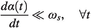
1. α(t) ≪ 1, ∀ tαt≪1,∀t
2. dαtdt≪ωs,∀t

Solve
We have then
Close to zero crossings, which we define similarly to the previous section where sin(ωst) ≈ ωs(t − tn)sinωst≈ωst−tn and cos(ωst) ≈ 1cosωst≈1, we get

For VsVs to be at a zero crossing we find

where the last step is just assumption 2 above. We can look at the time average (denoted by 〈⋅〉⋅) of the square of this expression

We have

where we define α′(t)α′t as α(tn)αtn in units of phase/time . We can finally use Parseval’s theorem and get

where α̂f has units radians/Hz
 and the single sideband noise (SSB) power, P(f)Pf, has units [radians2/Hz]. We then get

Evaluate
There is one particularly interesting thing to note about the derivation. The last term in (7.2) has units of voltage. Let us replace this with a voltage noise term vn(t)vnt instead, so we find
As before, for this to be at a zero crossing we find

where we have assumed the terms vnvn vary slowly compared with the main tone. We get

With this we see there is no way to distinguish the added voltage noise from the phase noise. We can look at the jitter phenomenon either as a phase noise or as an added voltage noise source. This is the root cause of the somewhat confusing units, as described earlier; we can view this spectrum as either a phase or a voltage for small phase deviations. Likewise, in modern simulators we can choose to calculate jitter from a phase noise integration or by looking at the voltage noise at the zero crossings. The two approaches should obviously agree. Note that this is, strictly speaking, only true when assumption 2 is valid. For large phase deviations we do not have correspondingly large voltage noise. Instead, the voltage noise has a natural limitation referred to as linewidth.
Finally, we note that when using the voltage noise domain approach, the voltage noise source transfers to jitter as

The denominator Aωs = dVs/dtAωs=dVs/dt. We find
 (7.3)
(7.3)Summary
The jitter–phase noise relationship is a simple calculation of the phase noise power in a sideband divided by the fundamental tone cycle frequency. A simple sinusoidal noise source is helpful when explaining the jitter–phase noise relationship.
7.3 Phase-Locked Loops
Phase-locked loops (PLLs) and various varieties of them are in common use in the semiconductor industry. These systems are discussed in many books, including [2–5]. See, in particular, [4] for an interesting nonlinear analysis. They are the key element when it comes to clock and timing generation, and many topologies are used to meet the varying key specifications that are needed. How to simplify these systems to study them analytically is generally known, and we will just present the basic theory here. The first sections describes architectures, performance criteria and common PLL sub-blocks. We then describe the general transfer function for a second-order, type 2 PLL, while the following sections describe detailed calculations of stability and noise transfer for a PLL loop. Finally, a design example is provided.
Architectures
Traditionally phase-locked loops have been divided into integer-N and fractional-N PLLs. The integer-N PLL features a simple integer divider, while the fractional-N PLL has some kind of averaging technique implemented in the divider that makes it possible for the loop to lock to a continuous range of frequencies.
Exciting PLLs have been invented recently, such as subsampling PLLs that circumvent some of the shortcomings of the established topologies.
Performance Criteria
DC Specifications
Power consumption: A key DC specification is the power consumption. In modern life, battery powered devices are very popular and keeping the power consumption low for all the circuit components is critical for market success.
AC Specifications
We describe briefly the most common AC specifications for PLLs here.
Loop bandwidth: the closed loop bandwidth is a key to stability considerations. If it is too wide, the phase detector discrete sampling operation will cause problems. Depending on the cleanness of the on-chip VCO vs the reference oscillator, one might choose wide vs narrow bandwidths.
Phase margin: key to loop filter design and stability.
Lock time: the time it takes for a PLL to lock.
Jitter: the accuracy of the resulting clock is important for ADC applications, as will be discussed later in the chapter.
Spur level: spurs from the reference clock can show up in unexpected places.
PLL Sub-Blocks
A traditional PLL consists of four basic blocks: a phase detector, a VCO, a frequency divider, and a filter: see Figure 7.1. In this subsection we briefly describe them and derive some simple scaling rules.

Figure 7.1 Traditional phase-locked loop topology.
Phase Detector
The role of the phase detector is to amplify the phase difference between two input square waves, referred to as the reference clock and the, possibly divided down, oscillator clock. It can be implemented in many different ways, and we will not go into all the possibilities here. Instead, we will take a brief look at a phase frequency detector followed by a charge pump implementation, depicted in Figure 7.2. It is a very common workhorse in the industry.

Figure 7.2 A functional view of a phase detector implemented as a phase frequency detector with a charge pump.
The flip-flops are usually up or down edge sensitive. Depending on which edge comes first, the upper or lower current source is turned towards the output where it sources or sinks charge from the next block, which is the filter block consisting of a capacitor to ground, for simplicity. When the edge from the opposite source comes into the phase detector, the currents are turned off from the output. In this way the difference in phase between the reference and the divided down clock is translated into a current pulse. We can define the gain of this block as

The phase difference can go from +2π+2π to −2π−2π.
The time it will take to bring the PLL all the way from its start-up condition to phase lock is known as the pull-in time. Let us do an order of magnitude estimate of this time using estimation analysis.
Simplify
First we assume the output of the phase detector sits at ground and the VCO is tuned such that the correct output frequency occurs when the control voltage at the input, which is the same as the phase detector output, is at power supply VDD, typically 7–900 mV in small geometry CMOS. The charge pump needs to bring up the output node all the way from ground to VDD. We know from our earlier discussion, on comparator analysis in Chapter 3, that this scales like

The analysis is somewhat complicated by the fact the charge pump is only on for a limited time and it is possible the edge order will switch during the pull-in stage, depending on the overall dynamics. We will ignore such complications here.
Solve
This is now simply a matter of plugging in the numbers, and we find

In the last step we use the initial offset in frequency instead of voltage as a measure of how far one needs to go.
Verify
This is similar to other discussions, so here we have allowed ourselves a few shortcuts to arrive at a number very similar to what others have derived (see [2]).
Evaluate
It is clear that a small capacitance and a large current are helpful if a fast pull-in time is needed.
Voltage-Controlled Oscillator
The voltage-controlled oscillator will be discussed in much more detail in Section 7.4. Here we will just define the basic characteristics. The easiest way to change an oscillator’s frequency is to change the effective tank load; in almost all cases this means changing a capacitance, and in most modern CMOS technologies this is natural to transistors. There are often specially constructed varactor devices with this particular property such that their capacitance is changing with its bias voltage. We can now define the gain of a voltage-controlled oscillator as KVCOKVCO and we find we have an output frequency
with a given input voltage VinVin; note the unit of KVCOKVCO is in angular frequency 2πf2πf [MHz/V]. The KVCOKVCO is assumed to be constant for estimation calculations, but in a real circuitry it will vary with voltage.
For PLL analysis we are interested in phase and not in frequency, which can often be a confusing difference. Let us think of a sine wave
The argument to the sinus function is a phase, but there is a frequency variable in the expression. Phase is defined as the integral of frequency. In our case in our sine wave we have a phase

In particular, for a time varying frequency this formula can be really helpful. We can now simply relate the input voltage to the oscillator to the output phase as
which in Laplace domain corresponds to a division by ss,

Frequency Divider
The frequency divider simply takes an input frequency and divides it by the desired factor NN. The corresponding change in phase is simply a division by NN. The gain is now

PLL Filter
We will discuss this block further in section “Fundamental Stability Discussion.” For now, we will simply describe it as a two-port system with transfer function F(s)Fs.
Basic PLL Equations
We can now pull all these block definitions together and derive the basic PLL equations. We will use the linearized transfer functions we derived in the previous section.
Simplify
We will consider a phase-locked loop as in Figure 7.3. It consists of an input reference signal, a phase detector (PD), a filter, a VCO and a divider circuit. The way to simplify such a system is to linearize all the blocks and assign a gain, or transfer function, to each one. These transfer functions for the various components are illustrated in the figure. Usually, the blocks are described in terms of Laplace transformations. In a typical application one is interested in the phase transfer in the loop, and all entities here refer to phase. The variable ss represents the modulation frequency around the nominal frequency. The linearization technique we describe here is known as the continuous time approximation where we ignore the fact that the phase detector–charge pump combination is actually a discrete time block. For this approximation to be valid, the loop filter bandwidth needs to be about 10× lower than the reference frequency.

Figure 7.3 Basic PLL topology with block gains.
Solve
We start by looking at the error signal,

We find explicitly,

We now find the transfer function T(s) = vo(s)/FinTs=vos/Fin from input to the VCO output
 (7.4)
(7.4)Verify
This is a well-known calculation and can be found in most textbooks on PLLs.
Evaluate
Depending on the filter, we see we have at least a first-order characteristic equation in the denominator of equation (7.4).
Fundamental Stability Discussion
Stability of feedback systems is a well-studied subject, for example in [6, 7]. It comes up in many discussions, and a good understanding is very helpful in day-to-day engineering work. Here we will discuss it in the special context of PLL and second-order transfer functions. We will make some simplifying assumptions that are common in the subject and we hope the reader will be inspired to do explorations on his/her own. In the literature stability is usually discussed in terms phase margin and gain margin using Bode plots and open loop responses. This presentation uses the closed loop response to study stability. It is hoped that it will provide new insight and some variation to the more common open loop analysis. We leave it as an exercise for the reader to examine stability using open loop response.
We will use the transfer function we derived earlier and look at a couple of specific examples of the filter function, F(s)Fs, and see what it implies about the system’s stability.
We have for the closed loop gain

Simplify
For the filter function we will need a low-pass filter, and since the output of the charge pump is a current, the simplest low-pass filter is simply

We find then

Solve
This is a two-pole system and we can find the poles with a bit of rewrite:

From Appendix B we see this has the time solution

Clearly, while it does not have any increasing amplitude with time, the loop will oscillate. In most definitions of stability this situation is referred to as marginally stable, although in practice it is not acceptable. The oscillation frequency is called the natural frequency

With this definition we find for

The stability situation is not so good and we need to do something about that, but first let us look at the bandwidth. By replacing s → jωs→jω and looking at the magnitude of T(jω)Tjω, we have

We see there is a singularity at the natural frequency. Let us look beyond that (denominator changes sign) and find the 3 dB bandwidth.


In this case, the bandwidth is a tad higher than the natural frequency. As a side note, it is interesting that among the real PLLs one can buy in the market, there is often quite a bit of peaking around the natural frequency. We will see shortly that this kind of response is fairly straightforward to correct.
Evaluate
The expression for the bandwidth is dependent on the filter coefficients.
From a stability viewpoint, the simplification we did here in which we had a simple capacitor as integrator is simply not acceptable. In order to improve the situation we need to add a real part in the left-hand plane to the poles. We will investigate this in the next section.
Improved Stability
The suspicion is now that our loop filter is too trivial. We just have a simple integrator, a capacitor. Let us attempt a more complicated one.
Simplify

where a > 0a>0. For low frequencies we retain our integrator action, but for high frequencies we have added a zero resulting in a constant output.
Solve
Putting this into our original transfer function, we find

Let us solve for the roots


Since a > 0a>0 we see we have been successful in our quest of creating a pole in the left-hand plane. Furthermore, we see we can get rid of any oscillation by choosing

This particular choice is referred to as a critically damped system. Let us put this choice into the transfer function and solve for the time behavior

We find from an inverse Laplace transform the impulse response is
There is a little bit of peaking and then the exponential roll-off.
This filter is simply a resistor in series with the capacitor. The input is a current and the output a voltage. We get

and

or
 (7.5)
(7.5)Finally, the bandwidth of the loop can now be estimated as


Evaluate
We have found a critically damped simple solution to our PLL model by making some simple assumptions and making them more complicated, to finally end up with a simple solution.
Summary
We have used estimation analysis to the full in this example and shown that we can derive some admittedly well-known results following the methodology.
Key Concept
A PLL’s stability can be improved by inserting a zero in the filter transfer function.
PLL Noise Transfer Analysis
Having derived the basic PLL parameters, we can now investigate noise transfer. The phase noise is particularly important when calculating jitter as we discussed in section “Phase Noise vs Jitter.” In this section we will discuss one noise calculation in detail and leave the rest as an exercise to the reader.
Noise Injected after the Filter
Noise injected after the loop filter can be estimated by simply adding in a noise signal as shown in Figure 7.4.

Figure 7.4 Basic PLL topology with noise injected after the filter.
Simplify
We simplify the situation by considering the various blocks around their normal bias point, so we can follow the situation described earlier.
Solve
Any noise injected after the filter will transfer as such:

Or,

We get at the VCO output

Evaluate
What does this mean? Let us go to various limits and observe the results, assuming F(s) = (1 + as)/(Cs)Fs=1+as/Cs. For high frequencies (large s) the second term in the denominator approaches a constant. This means the loop response to the high-frequency noise is simply a low-pass filter. For low frequencies, the second term in the denominator will dominate and the noise source n(s)ns will again be suppressed. In short, the loop acts as a band pass filter to the noise source.
Noise at the VCO Output Due to All Sources
Putting it all together, using the results from Exercise 7.1, we find at the VCO input the noise due to all noise sources in this simple model:

We can express these noise sources in terms of the PLL loop transfer function from equation (7.4).

These noise sources are uncorrelated and the resulting noise power can be written as

We see clearly the high pass function of the VCO transfer where most of the remaining blocks are low pass in nature.
Key Concept
A PLL transfer such as the VCO noise is high pass in nature, whereas the divider reference and phase detector are low pass in nature. Depending on the filter implementation, the filter noise response is often bandpass.
Example 7.1 Block design
Previously we discussed the basic equations determining the behavior of a PLL. We will here use them to define block specs for the individual blocks in the loop. This is an example of system design using the result of estimation analysis as a starting point. The fundamental parameters we derive can be put into a system simulator as a starting point for more detailed block-level specifications. Here, we will for brevity simply stop at the parameters provided by our simple model discussed in section “Basic PLL Equations.”
PLL Specifications
Table 7.1 Specification table for PLL
| Specification | Value | Comment |
|---|---|---|
| Output frequency | 25 GHz | |
| Input frequency | 2.5 GHz | |
| Output phase noise | −130 dBc/Hz | @ 1 MHz offset from tone |
| Bandwidth | 30 MHz |
PLL Block Definitions
From the specifications in Table 7.1 it is clear we need a divide ratio of 10. Let us look at the transfer function

We know N = 10N=10. It remains to define KVCO, CKVCO,C, and KPDKPD. For the charge pump we will choose a current of I = 1 mAI=1mA and a filter capacitance of C = 1 pFC=1pF. In a small geometry CMOS process we should have no difficulty with a 1 mA output current at 2.5 GHz. It is often better to use a higher charge pump gain than a high VCO gain due to the VCO sensitivity to the noise of the varactor. We can now look at the natural frequency and define the VCO gain.

Plugging in the numbers we find

This is a fairly reasonable number. We cover about 2.5% of the oscillator frequency and can make some adjustments for various center frequency shifts. We will use the KVCOKVCO we derived here as a key specification for a VCO design later in this chapter. With a series resistor in the loop filter, it now remains to find this resistance, which we do by choosing a critically damped system. We have from equation (7.5)

With these parameters we find the key parameters illustrated in Table 7.2.
Table 7.2 Parameters for PLL and noise spectrum
| Parameter | Value | Units |
|---|---|---|
| NN | 1010 | |
| KPDKPD | 1/2π1/2π | mA/rad |
| KVCOKVCO | 600600 | MHz/V |
| nrefnref | 00 | V |
| n(s)ns | 00 | V |
| nPDnPD | 1.2 ⋅ 10−121.2⋅10−12 | A/Hz |
| nVCO(s)nVCOs | 1/f1/f | V/Hz |
| ndivndiv | 9 ⋅ 10−109⋅10−10 | V/Hz |
| CC | 11 | pF |
| RR | 1010 | kohm |
A close-in phase noise response to the noise sources listed in Table 7.2 is shown in Figure 7.5.

Figure 7.5 Noise sources as a function of frequency offset in PLL. Note, no 1/f noise sources are included.
7.4 Voltage Controlled Oscillators
This section describes VCOs, and following the previous discussion of PLLs, we see that voltage noise at the input will translate to phase noise at the output. At the core of almost all high-performance integrated high speed oscillators is an LC resonator that determines the frequency of oscillation and often forms part of the feedback mechanism used to obtain sustained oscillations. In this section we describe how to solve for steady-state frequency, amplitude, phase noise, and finally a design example using estimation analysis. We base our discussion on references [6, 8–12].
Steady-State Frequency of Oscillation
The frequency of oscillation is naturally an important entity to understand when it comes to oscillators. We will calculate it with the help of estimation analysis.
Simplify
The analysis of a high-performance oscillator begins with an analysis of a damped LC resonator, such as the parallel resonator shown in Figure 7.6.

Figure 7.6 Simple model of VCO tank.
Since there are two reactive components, this is a second-order system, which can exhibit oscillatory behavior if the losses are low or if positive feedback is added. The values are fixed only at a given frequency. All the parameters vary with frequency, where the effective parallel resistance varies the most.
Solve
It is useful to find the system’s response to an external stimulus. We will solve this in two ways and show they are equivalent. First we will discuss a time domain solution, which we will use later. Then we will solve the same problem in the Laplace domain. First, let us look at the circuit in Figure 7.6 and analyze it using KCL:
 (7.6)
(7.6)We also know the inductor’s response to a change in current

We can this use in (7.6)

We now define

and we can rewrite
 (7.7)
(7.7)To solve these types of equation one can of course look up the solution in standard literature, but it is easier to work in the Laplace domain, which we will show shortly.
The general solution to this equation is

where A, BA,B are integration constants and can be determined from the initial conditions. The Laplace domain version of equation (7.7) becomes, by substituting d/dt → sd/dt→s


From the solutions we see the system’s response is a sinusoid with exponential decay as we found earlier. In order to maintain oscillation we need to periodically dump energy into this (tank) circuit. This is normally done by some kind of active amplifier, which is often modeled as a negative resistor in parallel with the tank.
Steady-State Amplitude Analysis
The amplitude of oscillation is set by the point where the energy lost during one cycle is equal to the energy supplied by the active circuit. The energy lost is due to the finite quality factor of the tank circuit. It has an equivalent shunt resistor in parallel, as discussed in the previous section. The energy supplied is determined by the average of the cross-coupled negative resistor from the active circuit. Here we will discuss how to estimate the amplitude using estimation analysis.
Simplify
We use as a simplification Figure 7.7. The problem can now be solved per harmonic, and here we will limit ourselves to the first harmonic only. In order to have a finite amplitude, the active circuit needs to be nonlinear to reduce the transconductance for high swing. If it does not, the amount of energy dumped into the tank will keep increasing. We will assume the active circuit current varies as such:
 (7.8)
(7.8)where both gm,gm″>0 . The negative first-order term is necessary to overcome the loss due to the real impedance in the tank, while the positive third-order term is necessary to limit the oscillation. The energy argument above means we need to find the amplitude where the absolute value of the time average admittance of the active circuit equals the time average admittance of the tank circuitry. The equation to solve is
where <>〈〉 denotes time average over one period.

Figure 7.7 Simplified model of oscillator with tank and active (nonlinear) circuit.
Solve
First we need to find the time average of the active admittance

where we used i(v)iv from (7.8). Expressing
we have the time averaged admittance

We now use

to write

since ∫0Tcos2ωtdt=0 .
.
Solving for the real total admittance of the oscillator now gives us

or
 (7.9)
(7.9)Evaluate
We see from equation (7.9) that the transconductance in the tank needs to be larger than 1/R1/R of the tank, otherwise no oscillation is possible. In addition, the third-order term, gm″>0 , needs to be small for the amplitude, AA, to be large, which is precisely what one might expect.
Phase Noise in Oscillators
Phase noise in oscillators has been studied in a number of papers over the years. Leeson’s model has historically been very popular. It is generally considered correct, but it involves certain fitting parameters, and roughly 20 years ago [12] provided an example of a physically based model employing estimation analysis similar to what we are discussing here. The theory is linear time variant (LTV). It is time variant because the effect of phase noise depends on when during the oscillation period the noise is injected (see Figure 7.8).

Figure 7.8 Noise injection for different phases. © [1998] Cambridge University Press.
The authors define what they call an impulse sensitivity function, Г(x), 0 ≤ x ≤ 2πГx,0≤x≤2π, where xx is varying over the oscillation period. It simply relates the phase response to a current impulse disturbance. It will be zero at the peak of the wave form and maximum at the zero crossing. In our simple VCO model we can calculate it fairly easily, and we can then use it to find the phase noise as a function of offset frequency. For the single sideband noise, they found
 (7.10)
where ГrmsГrms is the rms-value of the impulse sensitivity function, inin is the current noise being injected into the tank in units A2/HzA2/Hz, and ωω is the angular offset frequency. We see that if the current noise is white, the frequency offset will vary such as 1/ω21/ω2; if instead it varies as 1/f1/f, the phase noise will exhibit the well-known 1/f31/f3 slope. All these parameters are fairly easily understood with the possible exception of the impulse sensitivity function. To illustrate we will calculate it here in our simplified model of the tank. We start with the basic differential equation (7.7)

The delta function to the right is now due to an impulse current injected at time t = τt=τ.
Simplify
We can now use the fact that the effective resistance is infinite due to the cross-coupled transconductor providing an opposite resistance that cancels the loss. We have

Note, dimensionally [qn] = A sqn=As or ampere-second to work out properly. In other words, it is a charge.
Solve
The easiest way to solve these kinds of equations is to go to the Laplace domain and solve it there. We find

This is easily solved

This can be converted back to time domain and we find

For the voltage we now find

This is now a small disturbance added to the tank at t > τt>τ. Assume now the main oscillation is
If we now add the disturbance due to the injected current at time t = τt=τ we find

The perturbation term can now be identified with the impulse sensitivity function we were looking for, which can be illustrated with a couple of cases.
Verify
Let us look at specific values of ττ. If τ = 0τ=0 we have a simple sine wave with a zero crossing at t = 0t=0

which follows from a trivial trigonometric expansion. All the injected power goes into phase noise. If instead τ = π/(2ω)τ=π/2ω, we find

The injected noise is pure amplitude noise. This is all we can expect intuitively. Remember the forced units on qnqn [A s].
We see the perturbation term is very close to equation (7.10) and we identify
where 0 ≤ x ≤ 2π0≤x≤2π.
Evaluate
In summary, we find for the perturbation and its impact on phase noise with a charge impulse qnqn as a function of phase

where
where qmaxqmax is a normalization constant discussed in [12].
And for the rms value,
 (7.11)
For LC oscillators this expression will give us a good estimate of the magnitude of the noise.
Key Concept
A VCO’s jitter transfer is linear and time variant, LTV, in nature. In other words, the effect of noise on jitter depends on when the noise is injected.
Example 7.2 VCO design
We are now at a stage where a discussion of a VCO design is in order. We will build a VCO with bits and pieces we have designed in the previous chapters.
VCO Specifications
Table 7.3 shows the specifications for the VCO.
Table 7.3 Specification table for VCO
| Specification | Value | Comment |
|---|---|---|
| Output frequency | 25 GHz | |
| Gain | 300 MHz/V | = 1800 MHz/V in angular frequency. |
| Output phase noise | −140 dBc/Hz | @ 30 MHz offset from tone |
| Supply voltage | 0.9 V |
VCO Design
As we have discussed previously, a VCO consists mainly of some kind of resonant element, some kind of loop or a tuned resonant circuit, and an active element that replenishes the loss in this loop or resonant element. We will here use our results from the estimation analysis to:
Get a starting point of the design work from the estimation analysis;
Use this starting point in the simulator where we optimize the parameters.
This is a circuit example of how to use estimation analysis to speed up the design work. A good understanding of the basic behavior is essential to a good-quality end product. The simulator should not give us any surprises; it should just be used to fine-tune the performance, as we will discuss here.
We will focus on an LC VCO. We have two major design tasks. First we need to design the LC tank. We will draw from Chapter 5 to find an inductor with a specific Q. We will then shunt this with a capacitor from the same chapter to define the overall Q of this resonator at 25 GHz, which is the oscillation frequency. When we know the effective shunt loss resistor, we will be prepared to design the cross-coupled pair with a specific gmgm to overcome the loss. Generally, if we are using a fast enough process, the major headaches will involve the passive tank circuitry. We also need to isolate the output of the VCO from the load of the circuitry that follows. We will therefore use the CD stage we defined in Chapter 2 at the output. The topology we now have is illustrated in Figure 7.9.

Figure 7.9 Basic VCO topology.
Tank Design
To resonate, we need an inductor shunted by a capacitance. We learned in Chapters 4 and 5 that the inductance is set by the current pattern as it flows in a loop. It is therefore most important to include the full current loop, including the flow through the active circuitry, as shown in Figure 7.10.

Figure 7.10 VCO inductor including active circuitry showing AC current path loop.
Do not just include the coil itself. We have also learned that the resonance frequency is set to be the length of the inductor element, so we will attempt the design by having a single-ended inductor of
This gives a single-ended capacitance of

A rather large required capacitance is helpful in that the load on the tank can be included as part of the resonance. What will such an inductor look like? We created such a tank in Example 5.5, but the inductor in the tank was just the coil itself; now we need to include the connections from it to the active circuitry to get the inductance right. We will use a length of Lint = 40 μmLint=40μm, where the distance between these legs is d = 10 μmd=10μm. From equation (4.52) we find the added differential inductance due to the legs is

which is overestimated by about 30%, so we are off with the inductance by about 10%. The required capacitance is then 10% lower, or C = 0.36 pFC=0.36pF.
In order to adjust the frequency, a varactor needs to be included in the tank design. This device will change the capacitance and so the resonance frequency as a function of its bias voltage. From the specifications we see we need a gain of 300 MHz/V leading to a shift in frequency of 300 M/25 G = 1.2%300M/25G=1.2% variation, leading to a change in capacitance of 2.4%. The capacitance needs to change by 8.5 fF with one volt change. From the technology we find the varactor needs to have a size of roughly m = 2m=2.
Active Design
We now know the tank specs and can proceed with the active design. As a rule of thumb, the worst case is 1/gm < R/21/gm<R/2. This is to ensure we have enough margin to start the oscillations and to get a reasonable yield. We know the differential tank resistance RdiffRdiff from Example 5.5, from which we get the single-ended resistance RR and can thus calculate the transconductance needed

With this oscillator design we cannot use the thin-ox transistors due to over voltage stress. We instead use a 1.5 V unit transistor from our fictitious technology. From our tabulated transistor we then get a size of 10 fingers device from Appendix A. This transistor has a transconductance gm ≈ 6 mmhogm≈6mmho and should be enough to get the oscillation going.
Frequency: With these parameters we see that the capacitance of the active stage can be estimated using the calculation in Exercise 2.5. We find Cload, act = Cg + 4 Cd = 21 fFCload,act=Cg+4Cd=21fF. The tank capacitance should then be reduced to Ctank = 339 fFCtank=339fF. With the addition of the varactor, which has a nominal capacitance of 10 fF10fF per unit, we need two plus the load CD stage, which has an input capacitance of 9 fF9fF according to Example 2.1, so the final tank capacitor needed has an estimated size of Ctank = 310 fFCtank=310fF.
Amplitude: We have from equation (7.9) that the amplitude will be close to
A=gm−1R4gm″⋅3=5.8⋅10−3−133045⋅10−3⋅3=0.86VNotice that the negative resistance due to the “rotated” capacitor at the output of the follower, see Example 2.1, is negligible compared with the negative resistor provided by the cross-coupled pair.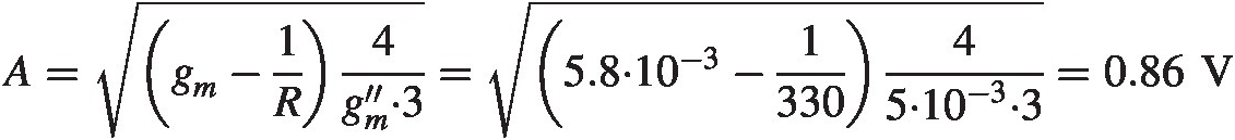
Phase noise: The expressions (7.10) and (7.11) show the phase noise to be expected is
ℒΔω=10logГrms2qmax2⋅in2¯/Δf4Δω2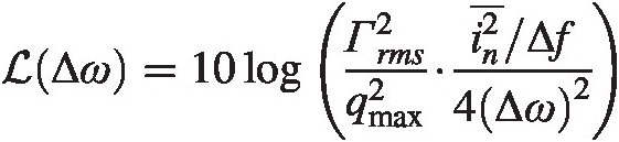


where


We assume here, and it is easy to verify, that the noise from the load resistor itself is small compared with the transistor noise. This is a single-ended expression. The differential impact on phase noise is 3 dB lower.
Finally, we have the estimated parameters/sizes for the components of the VCO in Table 7.4.
Table 7.4 Starting point parameters for VCO
| Device | Parameter | Value |
|---|---|---|
| Inductor | Inductance | 110 pH |
| Capacitor | Capacitance | 310 fF |
| Varactor | Multiplicity | 2 |
| M1, M2, medium thickness | W/L/NF | 1 μm/100 nm/10 |
Simulation
After implementing these sizes in the simulator, we find that the capacitance needed is underestimated, and a slightly updated table is shown in Table 7.5.
Table 7.5 Final sizes for VCO after simulation optimization
| Device | Parameter | Value |
|---|---|---|
| Inductor | Inductance | 110 pH |
| Capacitor | Capacitance | 315.6 fF |
| Varactor | Multiplicity | 2 |
| M1, M2, medium thickness | W/L/NF | 1 μm/100 nm/10 |
The main error in the capacitance is that we have assumed a full Cload, actCload,act at all times. In reality the load capacitance will vary over the cycle for all transistors.
After this has been sized, we confirm the operation with a simple simulation in Figures 7.11 and 7.12.

Figure 7.11 Oscillation frequency vs control voltage.

Figure 7.12 Phase noise of oscillator nodes.
From the figures it is clear our correlation is very good for higher offset frequencies. For lower frequencies the 1/f1/f noise of the transistors starts to come into play. Upon closer examination there are a couple of competing effects that cancel each other out. The transistor noise is overestimated, but it is compensated by the fact we do not include the other noise sources in the system, from the varactor and the tank resistance for example. The single-ended amplitude is ~710 mV as compared with our estimate of 860 mV, so we are around 2 dB off there.
Next Steps: The next steps in the development would be to run through all process, voltage, and temperature corners to make sure we meet the specifications everywhere. After that, a full layout including parasitic elements should be done. The size of the capacitor is likely to need some adjustment after the physical design is completed.
Summary: The main take-home point from this design example is to do one’s homework before simulating. A proper estimation analysis gives a great starting point for the simulation phase where, most of the time, we just need to fine-tune the sizing. However, be aware that VCO design is a rich subject with lots of available topologies and the performance criteria we have focused on here are just the very basics. For a thorough analysis of oscillator design, please see [14]. Having cautioned the reader properly on the limits of the analysis, we have demonstrated here that the path to deeper understanding lies along the route we have just taken.
7.5 Analog-to-Digital Converters
Introduction
Analog-to-digital converters (ADCs) are one of the key building blocks in today’s circuitry (see [15–19]). They are part of almost every large integrated circuit in one form or another. The reason is obvious: we live in an analog world, but our circuitry is mostly good at handling digital information, so one needs an interface between them. Over the years many different kinds of architectures have been invented, and we will just briefly mention them here. One common theme in all these systems is sampling, where a signal is looked at briefly and then converted into a digital word and then the process repeats.
This section will first discuss simple models of ADCs as a whole. We start with the most basic of models where there is no explicit sampler. We then continue with a simple model of a sampled ADC followed by a discussion of architectures, performance criteria and a design example.
The general discussion of ADCs is followed by a section on sampling. The effect of sampling can cause unexpected results to the uninitiated, and we will discuss how to simplify the analysis of the sampling process so that a clearer picture will emerge. We will start with voltage sampling, which is perhaps the most common, and continue with charge sampling, a somewhat less used technique. Incidentally, sampling can be viewed as an up–down converter and we will take a quick peek at this effect also in the exercises.
Basic ADC Model
Let us consider a simple model of an ADC and approach it with the estimation analysis we are discussing in this book. We will first make a simple model and see what we can learn from it regarding an ADC’s performance. In particular we will calculate quantization noise using this simple model.
Simplify
To avoid unnecessary details, let us assume we have a data converter that outputs signed integers in the range −2N − 1 + 1 → 2N − 1−2N−1+1→2N−1. This will result in 2N2N output levels. We further assume
1. The input to this ADC is a sine wave
fin = A sin ωt,fin=Asinωt,
where
A = 2N − 1A=2N−1
2. N ≫ 1N≫1 so that the input signal can be approximated with a straight line in between transitions.
The output of this simple model is now simply
The 0.5 comes from the assumption that the output is the closest integer level to the input signal. We will now see a step function response at the output as in Figure 7.13.

Figure 7.13 Basic ADC functionality.
Clearly the original tone is in there, but there are also other signals present. Let us find those
Figure 7.14 shows this graphically.

Figure 7.14 Close-up of ADC model output vs input at a transition point. The black curve is the input signal and the gray curve is the output signal.
The noise is simply a sawtooth function over the transition time that starts at 0, goes to −0.5 at the midpoint, t = tn + 1/2t=tn+1/2, where the transition occurs, which adds a 1 to the noise which is then reduced back to 0 at t = tn + 1t=tn+1. Mathematically we have

where we have used the Heaviside function θθ.
Solve
Let us calculate the power in one of these windows

Over a period, Δt = TΔt=T, we get a total noise

The power of the sine wave over the same period is simply

We have then a signal-to-noise ratio of

A more familiar form of this is the dB version

Verify
With N bits the quantization noise from an ADC is such that the SNR becomes
This is a well-known formula and can be found in pretty much all textbooks on ADCs. We see again that by making a really simple model of an ADC we can learn something fundamental about their properties.
Evaluate
When we discuss noise of an ADC, it is often dominated by the quantization noise. There is little point in making an ADC completely dominated by thermal noise since we can get similar performance simply by decreasing the resolution, which can lead to a significant reduction in design time (and power!).
Key Concept
The quantization noise of an ADC results in a signal-to-noise ratio of
ADC Model with Sampling
The basic model just presented has some obvious limitations, the most severe of which is that the sampling rate is dependent on the signal itself. This means it will be very difficult to find out its frequency content a priori, and the downstream processing will need to resample the output or some such scheme. It is also clear from the very simplified model just presented that in a real world ADC there is a finite time needed for the circuitry to convert the signal to a digital word. If this finite time is an appreciable portion of the signal period, the circuitry can quickly get confused and signal loss/distortion effects and other degradations can occur. The classic remedy for both of these problems is a uniform sampler in time, where the input signal is held for a certain amount of time, giving the circuitry a chance to convert the signal undisturbed. Sampling is almost always done at a fixed frequency and there are a number of ways to accomplish this with circuitry. We will study two such common methods in this chapter from a systems perspective: voltage sampling and charge sampling. The effect of sampling on a signal is of course well studied, but here we will include detailed calculations that describe the effect explicitly.
Nyquist Criterion
One effect that should be mentioned here is the Nyquist criterion, which states that with a given sampling frequency, fsfs, the signal needs to be within a bandwidth of fs/2fs/2. Curiously, this frequency band could be anywhere in the spectrum in principle. If it is within fs/2fs/2, it is referred to as the first Nyquist band. If it is between fs/2fs/2 and fsfs, it is within the second Nyquist band, and so on. We will derive a precise expression for this effect and its cause in section “Voltage Sampling Theory.”
Key Concept
Due to folding effects, an ADC needs to have its input signal band limited to within a bandwidth of fs/2fs/2 where fsfs is the sampling frequency.
In the rest of the chapter we will assume the signal is sampled with a certain constant sampling period, TsTs.
To model a uniform sampling window, one traditionally makes an additional assumption to the first two in section “Basic ADC Model.”
3. This signal is “active,” meaning two consecutive samples have different output words.
This assumption is needed to decouple the concept of noise power from the signal itself. Imagine a DC signal sitting right at the average trigger point. The output would then have no noise. If it sits right at the boundary, it will have maximum noise, 0.5 lest-significant-bit (LSB). The noise is then clearly signal-dependent. In a real system this is unrealistic since real world signals one encounters in practice are quite active. These three criteria are referred to as Bennet’s criteria (see [15]).
At each sampling point we now make the simplifying assumption that the quantization error is uniformly distributed over the range + 0.5 LSB shown in Figure 7.15 (see [15]).

Figure 7.15 Uniform transition probability.
We find for the noise power:

This is in effect the same calculation we did before, but framed a little differently.
SNR Improvement from Averaging with the Simple Model
Imagine we take the original system and sample it twice as fast, after which we average two consecutive outputs. The overall sampling rate has not changed but something interesting has happened. Let us investigate with a simple model.
Simplify
We will look at two consecutive samples, Si, Si + 1/2Si,Si+1/2. Each of these can be modeled as
where ViVi is the sampled signal and nini is the sampled noise. We will simplify by assuming the noise terms are uncorrelated in consecutive samples so their noise power will add up, and furthermore that on average the noise power is the same for all samples.
Solve
We find now after adding the two samples

After averaging we find the signal is

and the noise

The noise power is half of the original, or 3 dB in logarithmic terms, while the signal has the same power. The SNR has improved by 3 dB!
Evaluate
In general this is a very powerful method to improve SNR if you can handle the speed; each doubling of the sampling rate followed by averaging improves the SNR by half a bit.
or in dB
where KK is the oversampling factor.
Key Concept
The SNR of an ADC can be improved by oversampling followed by averaging.
Architectures
There are many ways to build ADCs. The modern literature contains a plethora of varieties and we cannot do them all justice here [15–19]. We will just mention some common ones and in the next few sections look at one or two in some detail.
Flash converter: This is simply an input stage driving 2N − 12N−1 comparators in parallel. It is the fastest architecture but it has serious size limitations, with every bit increase causing a doubling in size! It is unusual to find implementation higher than six bits and the power consumption it requires can be substantial.
Pipeline converter: The pipeline converter does the conversion in two steps, where each step has fewer bits and thus the combined resolution is higher.
Sigma–delta converter: This is a very powerful way to improve noise performance by up-converting it out of the signal frequency band. Upon low-pass filtering the resulting noise improvement can be dramatic. Its weakness is that it requires oversampling and can thus not be used in really high-frequency applications.
Time-digital converter: This novel idea uses counting of pulse widths to convert analog data to the digital domain. It employs such fancy circuit techniques as time-amplifiers [16].
Successive approximation register (SAR): This implementation does one-bit comparison per sampling clock. It is not a very fast architecture but is extraordinary low power since it is almost exclusively digital in nature.
Time-interleaved converters: This architecture is a combination of sampling + multiplexer + slower ADCs in the back. For modern high-speed data converters it is the most common architecture employed. The slow backend ADC is usually a SAR.
In this chapter we will study an implementation of a flash ADC and look in more detail at the peculiarities of a time-interleaved system.
Performance Criteria
There are many ways to characterize a data converter (see, for example, [15–19]). The application determines which ones should be used. Here we will mention just a few common ones, and for the rest of the chapter we will use the signal-to-noise ratio as the performance criterion.
DC Specification
Resolution: This is the number of output bit lanes for ADCs. It does not necessarily relate to the accuracy of the converter.
Integral nonlinearity (INL): This is the deviation of the output code from a straight line drawn through zero and full scale when the input is a straight DC ramp.
Differential nonlinearity (DNL): This describes the difference between two adjacent code outputs compared with an LSB step size.
Offset: Matching of components is far from ideal in modern integrated circuits. Mismatch effects will cause offset as referred to the input signal. A zero at the input will result in a nonzero equivalent at the output.
Power: The power consumption is often a very critical specification when circuitry is used in battery powered devices.
AC Specifications
The AC or dynamic specifications are often the most highlighted ones, given their reputation as being the hardest to meet. This is often the case, but the same weaknesses can usually be found in the DC specifications.
Signal-to-noise ratio (SNR): This is simply the ratio of the signal power to the power of everything else, excluding harmonic distortion.
Total harmonic distortion (THD): This is the sum of all harmonic powers divided by the power in the main tone, expressed most commonly as a percentage (%). We will use THD in dB.
Signal-to-noise and distortion ratio (SNDR): This is simply the ratio of the signal power to the power of everything else, including harmonic distortion.
Effective number of bits (ENOB): The definition of ENOB is somewhat confusing. There is a formal IEEE definition, but most current literature uses a simpler one defined as
ENOB=20logSNDR−1.766.02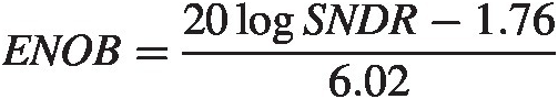
Spurious-free dynamic range: This is the difference in dB between the main tone and the highest spur in the spectrum.
Bit error rate (BER): This the ratio of conversion errors over the number of conversions done: see Chapter 3.

In most modern papers describing ADC performance the discrete Fourier transform of the output signal is used:

One can use this formula to investigate issues such as SNR, SNDR, THD, and other such issues that occur with reasonable frequency. Things such as 1/f noise, and glitches including missing codes, either require excessive sampling times or need to be investigated with other means. Using these kinds of transforms can be very revealing of the system’s performance. Be on the lookout for odd noise floor behavior, and unusual output signal power. These can be indicative of unhealthy circuit behavior. If the capture time is not long enough, the detrimental effects of jitter can be hidden in the main tone. Apart from some of the rare defects mentioned previously, the Fourier transform of the signal is very revealing of the full circuit behavior.
For our purposes we will use SNR, SNDR, and THD as key specifications to illustrate the use of estimation analysis in the design of data converters.
Interleaving ADC
Many modern high-speed ADCs use time-interleaving topologies to achieve high sample rates. An example is shown in Figure 7.16.

Figure 7.16 Time-interleave topology.
The idea is to mux the input sampled data to several slower-speed ADCs that output their data in a synchronous manner. This output is aligned timing-wise to achieve the designed sample rate. Various imperfections in the slower-speed ADCs will affect the output result in predictable way, and we will study a simplified version of such an ADC in this section.
Simplify
We make the simplification that there are only two time-interleaved data paths. We will first look at the effect of offset differences between the two digitizers followed by a discussion of gain mismatch. We will also assume there is no thermal noise to worry about.

If we plot this, we find as illustrated in Figure 7.17.

Figure 7.17 Figure showing offset effect. The two dashed curves indicate the offset of the two ADC slices.
Solve
We can now Fourier transform this effect:

In addition to a sinusoid sampled with a period TT, there is a DC tone sampled with a 2 ⋅ T2⋅T period that will appear at frequencies, m π/Tm/2T, half the sampling frequency. This is simply the up-converted version of the offset in one channel.
The effect of gain mismatch can be analyzed similarly: see Figure 7.18.

Figure 7.18 Figure showing gain mismatch effect. The two dashed curves indicate the gain of each ADC slice.
We now have

We have a sinusoid sampled with a period TT and a sinusoid, with amplitude given by the gain mismatch, sampled at half the sampling frequency. This second term will give rise to tones at m π/T ± fsm/2T±fs.
Evaluate
In general for an n-interleaved system, any offset will show up as spurs around Fs/nFs/n, and any gain mismatch will show up at Fs/n ± fFs/n±f.
Summary
We have studied simple ADC models and realized some relevant properties by using estimation analysis. Although most of these results are well known, it is hoped that the reader will be encouraged by the methodology used and will be inspired to explore ADCs and their properties on his/her own. By simply pondering the systems under consideration and trying to capture their essence through simple models, much can be learned on one’s own.
Example 7.3 Flash ADC design
Since we have discussed a few basic examples of key ADC components, let us put together a flash ADC. This is arguably the simplest and, as such, the fastest of the traditional topologies and will serve as a good example of how to use the estimation analysis to design circuits. It is not necessarily the most power conservative topology, and for such applications where power is paramount the ADC literature has plenty of examples of efficient architectures. Due to space limitations we will only consider a few of the normal specifications here. A full ADC design requires specifications on effects such as offset and power consumption and others that we will leave to the side here. One can, however, easily incorporate these other effects using estimation analysis techniques.
ADC Design
We will use here the results from the estimation analysis we have done with several circuits along the way in this book, in particular from Chapters 2 and 3, to:
Get a starting point of the design work from the estimation analysis
Use this starting point in the simulator where we optimize the parameters
This is another circuit example of how to use estimation analysis to speed up the design work. A good understanding of the basic behavior is essential to a good-quality end product. The simulator should not give us any surprises; it should just be used to fine-tune the performance, as we will discuss here.
The topology we will use is shown in Figure 7.19. The first block is an anti-aliasing filter that simply ensures the signal coming through to the ADC has the signal limited to the appropriate Nyquist band. This block will not be discussed here at all; instead, we assume the input signal is properly band limited.

Figure 7.19 Basic ADC topology.
We will take the input stage, the follower, from Chapter 2, the buffer and comparator from Chapter 3, and for the sampling switch we will first not use any and then compare the bandwidth to the case where we use an ideal one with a series resistance.
One important issue we have not touched upon when designing the comparator is the kickback phenomenon. The tail reset switch in Figure 3.3 will cause the source voltage of the differential pair to move to ground node vss rapidly. This rapid change in voltage will induce a current through the gate source capacitance of the input transistor and into the driving impedance of the input source.

This will induce a voltage that will interfere with the precious input signal and can cause significant problems. A simple scaling argument shows

One is helped to some degree by the differential operation of the circuitry, but if one needs high precision, it may very well be insufficient.
A preferred way to deal with this is to use a preamplifier to isolate the comparator kickback from the input signal. It will also help with offset, but it will cause additional delays and at times it may be unacceptable. One can also use different, higher power, comparators where the circuit is biased the whole time. Here we will use a preamplifier from Example 3.2. We have the topology as outlined in Figure 7.20.

Figure 7.20 Straight flash ADC topology.
The circuit blocks have already been designed with this system specification in mind, and upon putting everything together and simulating we find the following set of results for different frequencies. Note, for these simulations nothing was changed compared with the earlier circuitry. Everything was designed/estimated with proper driving source/load impedance and so no adjustments were made! The resulting spectrums for two separate input tones are shown in Figure 7.21. The final results are shown in Table 7.7.

Figure 7.21 Output spectrum of flash ADC at 100 MHz and 6 GHz.
Bandwidth Estimation
We define the bandwidth as the response at the output of the bottom resistor in the string. The bandwidth is set by two properties of the system, first the CD stage output driver and then the fact that we do not use a sampling switch here. These two facts will limit our bandwidth. The aperture window for the comparator is really short, a few ps from our discussion in Chapter 3, section “Comparator Analysis,” so it will not impact the bandwidth. The CD stage consists of a string of low-ohmic resistors driving the capacitive input stage of the preamp. There are 63 such RCRC time constants and the accumulated effect is more significant than just 63 ⋅ RC63⋅RC, since the filters are loading each other. Instead, we can employ estimation analysis to get an idea of the bandwidth.
Simplify
Let us approximate the system with a one-pole system, with a resistor equal to the sum of all resistors and a capacitance equal to the sum of all capacitances, where we use a fixed C = 12 fFC=12fF from Example 2.2. The resistor is given by design Example 2.2 plus the follower output resistance 1/gm = 12 ohm1/gm=12ohm. This will give us a lower bound on the bandwidth.
Solve
The estimated bandwidth is simply

Verify
The simulated answer for the RC network itself is
In the full simulation with active circuitry we find the bandwidth slightly lower due to higher effective capacitance, and we end up with
Figure 7.22 shows something interesting. First, Figure 7.22a shows the gain response as we have described it here with a 3 dB point at about 7 GHz. Figure 7.22b shows the same simulation with an ideal sampling switch (10 ohm series resistance) at the gate of the input stage transistor. Here the bandwidth has improved dramatically! The reason is that the resistive ladder now has time to settle since the input is being held for roughly half the sampling period. We will not go into the details of real sampling switch implementations here but hope the reader will be inspired to explore on her/his own.

Figure 7.22 Gain transfer function vs input frequency; the frequencies above Nyquist have been measured as the folded down frequencies. The input signal is 1 dB backed off full scale. (a) The gain without an input sampling switch, and (b) the gain response with an ideal input sampling switch in series with a 10 ohm resistor.
Distortion Estimation
The distortion will be dominated by the input CD stage. We have seen in Chapter 2 that with a sufficient load, the distortion of a CD stage will be small. In our case we have a large impedance due to the current sink, about 1 kohm, and from the second and third harmonic terms calculated in Chapter 2, Section 2.2 and Example 2.2 we see that the third harmonic term should be

In other words, it is completely negligible. This was also confirmed by simulating low frequencies <100 MHz. For higher frequencies we see from the plots there are some distortion terms showing up, but they are small and will not degrade SNDR by much in this case.
Noise Estimation
The noise is best estimated at the input to the preamplifier. We know from Example 3.1 that the input noise to the comparator is

The preamplifier’s output noise is roughly

These two noise sources are uncorrelated, and knowing that the preamplifier gain is around 2, we find the total noise at the preamplifier input to be

We need to compare this voltage to full scale ADC input, which is 800 mVppd or

Finally, the signal-to-thermal-noise ratio is then expected to be

Thermal noise should not be a limiting factor for the performance. We see also from the simulation results that the nonquantization noise is contributing roughly 0.5 dB.
Jitter Impact
We can consider the jitter from the PLL system we designed in Section 7.3. From Figure 7.5 we can estimate a jitter of around 10 fs, but that does not include 1/f contribution at low-frequency offset. Including these sources, the best jitter performance reported in the literature is around 50 fs. Let us assume we can match this number and see what the jitter impact would be on our ADC. At the first Nyquist boundary, we find

which is much smaller than the quantization noise. However, at the third and fourth Nyquist bands we may get into trouble if the signal loss is otherwise contained.
Conclusion
We have taken a brief look at the design of a flash ADC. The reader should be aware that a complete ADC design involves far more details. Criteria such as power, offset correction, layout parasitics, error detection, and many others must also be considered. Still, the exercise serves as an example of what one can do with simple estimation analysis. Other important issues can be addressed in the same way. Of particular interest is that the sizing of the various blocks was not changed in simulation; everything had been set up with the correct load and source impedance, and the sizing we had estimated and sometimes verified earlier was correct. So the circuitry worked! This was, of course, a simple example, but imagine the benefits on a larger scale.
Voltage Sampling Theory
Sampling a signal for later digitization is one of the most common operations in any modern IC. How sampling works with up-conversion folding and so on can often be challenging for engineers new to the field. We will use our modeling strategy to shed some light on this phenomenon.
To sample a signal, a precise clock source is used. The quality of the clock source is often described in terms of its jitter, and we will begin this section with a brief discussion of how jitter degrades the signal-to-noise ratio for voltage sampling. We follow this with a discussion of voltage sampling using an ideal switch, where concepts such as impulse sampling, track and hold, and so on are defined. This will help us work out some basic mathematical tools we can use for the noisy sampling study in the second section. The simplifications we will use will be stated in the beginning of each subsection and applied to several different subsequent situations. The purpose here is to illustrate how to create simple yet relevant models with some common examples, and in so doing we will present mathematical techniques in some detail.
Jitter
The degradation of signal-to-noise ratio due to jitter in the voltage mode was discussed in section “Phase Noise vs Jitter,” where we showed that the equivalent voltage noise follows the well-known jitter “ohms” law (7.3), illustrated in Figure 7.23. We find after some trivial rearrangement that the signal-to-noise ratio of jitter due to voltage sampling is
 (7.12)
Figure 7.23 Jitter impact on voltage sampling.
Fourier Transforms
In sampling theory we will work with Fourier transforms, and there are a few things worth mentioning before we start. First, we will look at a sampling situation with a fixed sampling period, TT. This means we should define the Fourier transform as
 (7.13)
where ω = 2πfω=2πf.
Second, we will work with both positive and negative frequencies. For real-valued functions h(t)ht the following property is easy to prove:
where * denotes the complex conjugate. For practical calculation we will usually study the positive frequencies and simply keep in mind that the negative ones are the complex conjugate of the positive. It is much easier to work with calculations this way.
Third, instead of using functions such as sinωtsinωt one should use Euler’s formula for sinusoidal functions:
From this we see
 (7.15)
Working with ejωtejωt functions is much easier when calculating Fourier transforms, as should be clear from the definition (7.13).
Working with “negative” frequencies can be a little confusing at first, so let us illustrate how it works with a simple example. Assume we have a function

where we need to calculate its power. From the basic definition we find the average power is

This is all well known. Now let us take the Fourier transform and look at the spectrum
 (7.16)
where we have used the continuous time definition of the Dirac delta function:

We see here we have two frequency tones at ω = ± ωsω=±ωs. Adding their powers, we should end up with the same expression PP above:

To summarize:
1. When working with negative frequencies, the tones on the negative frequency side are the complex conjugate of their positive frequency counterparts. We can simply stick to integrating the positive frequency power and multiply the result by two.
2. Alternatively, if we know the power density for positive frequencies, such as resistor noise, we can extend to negative frequencies by simply dividing the power density by 2 and mirror it along the ω = 0ω=0 axis.
Armed with these ground rules we can start.
Ideal Sampling Switch
For this section we need to know a couple of Fourier transforms that are helpful, as well as a couple of theorems. We start with something with which most readers will be familiar, impulse sampling, and we continue with track and hold and sample and hold sampling.
Simplify
The simple picture we will use throughout the section is pictured in Figure 7.24.
1. We model a sampling switch as an ideal switch in series with a resistor with zero ohm, Rs = 0Rs=0. The loop is completed by a (sampling) capacitor and a driving voltage source.
2. We will also assume for simplicity throughout this section that the on-time is half of the switch period.

Figure 7.24 Showing ideal sampling switch.
Solve
With these simplifications we will calculate the Fourier transform for two different situations: impulse sampling and track and hold sampling.
Impulse Sampling
Imagine we sample an input sine wave at certain equally spaced points in time only: see Figure 7.25.

Figure 7.25 Impulse sampling.
Mathematically, this can be expressed as multiplying the input with a series of delta functions:

where TT is the sampling period. As it stands, it is not very informative. We need to take the Fourier transform to learn more, and in order to do this we first need to take the Fourier transform of the sum of delta function so we can use the convolution theorem (see Appendix B). We have

The key observation here is that these terms will be zero unless:
The effect of this is a replacement of the sums

We then find

Now we are ready to use the convolution theorem, and we have for


These delta functions will appear over and over again, so to minimize the clutter we will use the following short forms:


We then have

We have an impulse train with tones of size A/2A/2 around all harmonics of the sampling frequency, as in Figure 7.26. We will see the same kind of calculation again and again all through this section; see [15] for similar discussions.

Figure 7.26 Spectrum of impulse sampling.
Track and Hold Sampling
Track and hold is a sampling technique where the input signal is visible at the output with some periodicity. The rest of the time the signal is held at a sampled value: Figure 7.27 shows an example. We will first discuss the Fourier transform of the track phase. The hold phase is simpler technically and we leave it as an exercise to the reader. The sum of the track and hold phases gives finally the track and hold result. As a bonus we will also present the sample and hold result.

Figure 7.27 A track and hold picture.
Fourier Transform of the Track Phase
The track phase can be viewed mathematically as a multiplication of signal by a square wave with amplitude V = 1V=1. Such a square wave has the Fourier transform:

The Fourier transform of the track phase
is now:

We see here that even integers cancel out (except n = 0n=0). We end up with

Fourier Transform of a Track and Hold Signal
We leave the hold phase to the reader as an exercise, and when putting all this together in one formula we get

and the result can be seen in Figure 7.28.

Figure 7.28 Frequency domain representation of track and hold signal. The track phase is indicated in thick black and the hold phase is given by the dashed line. The track and hold responses are offset slightly from each other to show the response more clearly. The overall sinc function is drawn in thin black.
Sample and Hold Sampling
Sample and hold sampling is similar to track and hold sampling, but the signal is not visible at the output directly; instead, it is held constant after sampling, and depending on the situation it returns to zero after some time or it is held all the way up to the next sample. In this section we calculate the case where the signal is held until the next sample. We leave the more general case to the reader as an exercise.
Fourier Transform of a Sample and Hold Signal
A sample and hold signal where the signal is held constant until the next sample is simply Fhold(ω)Fholdω with the hold period equal to the sampling period. We can simply do the substitution T → 2TT→2T for Fhold(ω)Fholdω in exercise 5 and we end up with

A picture of the spectrum in shown in Figure 7.29.

Figure 7.29 Frequency domain representation of sample and hold signal. The overall sinc function is drawn in thin black.
Verify
We have studied here some of the basics of sampling and sampled signals. We have seen how, with some basic Fourier series analysis, we can demonstrate a wide range of phenomena. The results presented can be found, for example, in [15].
Evaluate
The sampling effect can be simply estimated via Fourier series.
Noise Sampling
We have been looking at the basic sampling effects from a simple perspective, that of a single tone being subject to ideal sampling. What happens if you sample a circuit with noise? We will consider a refined sampling model where there is a noisy resistor in parallel with a capacitor as in Figure 7.24 with the switch permanently closed.
Lossy Resistor in Parallel with a Capacitor
Let us consider the following situation: a resistor in parallel with a capacitor to ground. The voltage source in Figure 7.24 is vs = 0vs=0, so the end of the resistor goes to ground and we will study the noise transfer, due to the lossy resistor, of this system to the capacitor when we sample the output node. It is perhaps as simple as one can make it. First, let us study this system without sampling. We can consider a noise voltage sitting in series with the resistor. We find at the capacitor
 .
.Since the noise is better known as a spectrum, we will look at the above in frequency space.

The resistor noise is white, and we can now integrate the noise power over frequency to find

where we have used

v˜n2 is defined over negative frequencies, so the power is half the normal textbook version. This is all well. What happens if we sample this system?
Let us assume at time tt the capacitor has a voltage v(t)vt, the input is

and the voltage on the capacitor is governed by a differential equation derived from

We find

A simple rewrite shows
 (7.17)
This is a first-order differential equation that has the solution
 (7.18)
We take the Fourier of v(t)vt and find, with B = 0B=0 (we assume the initial transient is negligible),

Ideal Impulse Sampling
Let us sample this with an ideal impulse sampler, where we again use the convolution theorem.

This simply means the spectrum with a specific sine wave source is shifted around each sampling frequency harmonic. Imagine now that we integrate ωsωs over all spectrum, in other words we have a white noise source with noise density A = 2kTRA=2kTR. We find


Figure 7.30 shows that by looking at ω < π/Tω<π/T, the first Nyquist zone, we see that noise contributions from higher harmonics of the sampling clock extend into the first Nyquist zone. We see that even though we restrict ωω to be within the first Nyquist zone, contributions from all harmonics extend into the first Nyquist zone, leaving the total integrated power in the first Nyquist zone equal to the total noise integrated over all frequencies without sampling. In fact, the same can be said about any Nyquist zone. All Nyquist zones contain all noise power in the ideal impulse sampling case. For a sample and hold situation, it is a little bit different, something we will explore next.

Figure 7.30 First three terms of |V(ω)|Vω. Within the first Nyquist zone the noise from the m = +1,2 terms are added to the noise, resulting in an increase in the total noise. The dashed lines indicate harmonics of the sampling frequency and the dash-dotted line the first Nyquist zone.
Finite Pulse Width Sampling
Let us sample this with a square wave where the switch is on for a time Ts/2Ts/2 and the rest of the time the output is zero.

After integrating the noise source again, we find the following spectrum

This expression is very similar to what we had before, with the exception of the absence of every even sampling harmonic, except DC.
Evaluate
With ideal impulse sampling, all Nyquist zones contain all noise power in the unsampled system. Finite sampling width results in a notch filter effect excluding some noise around some harmonics of the sampling frequency.
Key Concept
With ideal impulse sampling, all Nyquist zones contain all noise power in the unsampled system. Finite sampling width results in a notch filter effect excluding some noise around some harmonics of the sampling frequency.
Charge Sampling Theory
Charge sampling is a less frequently used technique to sample a signal. It was first proposed a few decades ago and although the utilization of this technique is not that extensive, it has some advantages that are worth discussing. We will follow [21] in the beginning and extend that discussion to more general situations. Since this technique is used less often, we will spend quite a bit more time on the mathematical derivations. We will use estimation analysis and start with some simplifications, followed by the now familiar Solve, Verify, and Evaluate discussions.
Simplify
Let us consider an ideal charge sampling model starting with the discussion in [21] and Figure 7.31.

Figure 7.31 Ideal current switch.
We will further simplify the discussion by assuming S1 is always on and S2 is an ideal switch that clears the capacitance in no time, with a period TsTs. When looking at a sine wave, we then have current integration from a time, tntn to a time tn + 1 = tn + Tstn+1=tn+Ts: see Figure 7.32.

Solve
Using
we find the sampled charge

where we have defined, A = I0 ⋅ TsA=I0⋅Ts, as the charge amplitude. Using
we get:
 (7.20)
We see here that for low frequencies we recover the sampled signal. For higher frequencies there is a roll-off determined by the last sine factor. At Nyquist, ωTs = πωTs=π this roll-off has an amplitude of A ⋅ 2/ωTs = A 2/πA⋅2/ωTs=A2/π or −3.9 dB loss compared with DC.
When jitter is added into the picture we get:
where
we get:

Assuming, ωσn ≪ 1ωσn≪1, we arrive at

For low frequencies ωTs ≪ 1ωTs≪1 we can now make an interesting observation,
 (7.21)
The first term is the original signal, while the last two show jitter contributions. Note that if the jitter components are correlated, σn + 1 = σnσn+1=σn the second term disappears and we have the usual jitter relationship from voltage sampling where the aperture jitter component is proportional to frequency (or the derivative of the signal). One can think of correlated jitter as a low-frequency drift of the sampling point: see Figure 7.33. For anti-correlated jitter σn + 1 = − σnσn+1=−σn, the third term disappears and we are left with jitter terms that can be called amplitude jitter in that they peak when signal amplitude peaks, shown in Figure 7.34. For uncorrelated jitter, both the second and third terms will contribute, and for small frequencies the second term is the dominant one. We have jitter effects even at DC.

Figure 7.33 Low-frequency drift of charge sampling points. Correlated sampling points. The distance between the sampling points is correct but the average charge sampling time is off by sigma. This situation typically occurs in low-frequency drifts.

Figure 7.34 Anti-correlated sampling points. The average charge sampling time is correct but the distance between the sampling points is off, causing the slice gain to be off. The odd and even sampling pulse edges move opposite each other.
Another way to think of this is in terms of differential signals. Any charge sampling event can be characterized by either the start or end time of the sampling interval or the common mode time (average) and the differential time. In other words, we can describe the sampling as a correlated signal plus an anti-correlated signal. These two signals can obviously vary with the sampling time.
For general frequencies we can also calculate the response
 (7.22)
where
 (7.23)
Evaluate
We have identified a couple of different modes of operations, and we will discuss them each in turn. We start with the correlated jitter and follow this by the anti-correlated jitter discussion.
When the jitter is correlated we get:
 (7.24)
which is very similar to the main tone except the phase is off by 90 degrees. In other words, it looks like phase jitter. To get the signal-to-noise ratio we need to convert to power and average signal and power over time, TT:

If we now define an effective jitter function
 (7.25)
 (7.26)
we see the same roll-off vs frequency as the signal.
For the signal we will also define it similarly
 (7.27)
We get for
 (7.28)
This is same expression one would get for pure voltage sampling; see earlier discussion, equation (7.12). Another way to look at this situation is to see that the sampling instance is off by σnσn and if the jitter is slowly changing, the next sample will be off by a similar amount.
Let us look at the opposite situation where jitter is anti-correlated, σn ≈ − σn + 1σn≈−σn+1, and the odd and even sample pulses are moving opposite each other.


We see in general that we get a sequence of samples with alternating sign
 (7.29)
For simplicity, let us assume σn = − σn + 1 = σσn=−σn+1=σ. We see then that this sequence is generated by multiplying the tone by a square wave with period 2Ts2Ts. The result is a tone at 1/(2 ∗ Ts) − ω/(2π)1/2∗Ts−ω/2π. In other words, the main tone gets no broadening of its profile. This situation is simply one of timing mismatch between odd/even samples, which will create a tone that looks like an interleave gain error around which the jitter noise moved. The cosine term in the previous expression shows that, close to Nyquist, this term is suppressed.
We can now go through the same calculation that led us to the correlated noise power, NcorrNcorr. We find
 (7.30)
And
 (7.31)
For low frequencies we see the expected dc value, (Ts/2σ)2Ts/2σ2, while for high frequencies we get ~1/(ω − ωs)2~1/ω−ωs2, which is a remarkable improvement! The improvement in noise is
 (7.32)
We see this ratio is less than 1 above Nyquist/2.
Key Concept
Anti-correlated jitter could provide significant improvement to SNR at frequencies above Nyquist/2.
For correlated noise, we get no benefit compared with voltage sampling! For anti-correlated, we get infinite benefit for the tone proper, although the total noise power only rolls down when the main tone is close to Nyquist – still a remarkable improvement in SNR. For uncorrelated jitter, half the jitter will be in the correlated and half will be anti-correlated. We find the total jitter power
 (7.33)
As the tone frequency changes, the sum of the contributions from the correlated and anti-correlated portions is the same but their relative power changes. For low frequency the anti-correlated jitter is dominant, while for high frequencies the correlated jitter dominates. This noise power can also be found directly from the expression for JnJn. We find, noting that both edges contribute equally to noise power,
 (7.34)
where we have, similarly to (7.25), defined an effective σσ. And we find
 (7.35)
The improvement for uncorrelated edge noise compared with correlated noise is:
 (7.36)
which shows that when (1/2)ωTs > π/4 → f > 1/4Ts1/2ωTs>π/4→f>1/4Ts we have an improvement of up to 3 dB at Nyquist. Since we still have jitter at DC, there is a penalty for low frequencies compared with correlated noise.
Verify
These two correlation models were simulated with the aid of a Matlab script, and the comparison is shown in Figures 7.35–7.37. We use a simple sinusoidal jitter tone that moves the integration edge up and down in time, similar to the model in section “Phase Noise vs Jitter.”

Figure 7.35 Matlab simulation of correlated charge sampling jitter and comparison with the estimated model.

Figure 7.36 Matlab simulation of anti-correlated sampling jitter and comparison with the estimated model.

Figure 7.37 Matlab simulation of uncorrelated charge sampling jitter and comparison with the estimated model.
Evaluate
The interesting thing to note here is that the anti-correlated signal-to-noise ratio can be significantly higher with the anti-correlated noise at high frequencies. For low frequencies, due to the roll-off of the noise power, it is still better than the correlated noise jitter. This promise caused some excitement early on when it was proposed. However, there is an assumption being made. If we look again at the phase noise response of a typical PLL, in Section 7.1 we found most phase noise was concentrated around the carrier. This causes slow movement of the carrier phase as a function of time. In the context of charge sampling, this means that almost all the jitter is correlated and the SNR degradation due to jitter is more or less identical with voltage sampling. Any portion of the jitter that is uncorrelated will give rise to jitter degradation even for a DC signal. If we can accept the DC degradation, we still need a PLL structure that can spread the noise out so it becomes white or uncorrelated, or we can create a topology that implements an anti-correlated jitter transfer – none of which is obvious, but it is worth some thought.
7.6 Summary
This chapter has explored clock generation in terms of PLLs and its implication in terms of sampling and analog-to-digital converters. We have studied this in the case of jitter in terms of both voltage sampling and charge sampling and have found some interesting relationships, all using simple modeling and estimates followed by verification in terms of literature or simulations. In addition, a few design examples were discussed where the estimation analysis was prominent, and we highlighted how such groundwork can lead to much better understanding of the system and therefore much faster design time.
7.7 Exercises
1. Derive the noise transfer from the VCO, divider, input reference signal, and phase detector block.
2. The open loop response, O(s)Os, for the PLL system in Section 7.3 is defined as
Os=FsKVCOKPDsN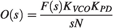
Use this expression to estimate phase margin, defined as the phase of O(jω) + 180Ojω+180at the point ωω where |O(jω)| = 1,Ojω=1, for the case where
a. Fs=1sC
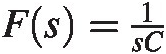
b. Fs=1+assC
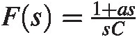
3. You are given a clock reference that has an extraordinary amount of phase noise spread out over the frequency close to the tone. How would you design a PLL that can clean up this noise?
4. You are given a VCO that has very poor phase noise performance. How would you specify the reference clock noise and the PLL bandwidth to fix this?
5. You are given an n bit flash ADC. You are asked to use its components to build an n + 1 bit flash ADC. How much would you expect the power consumption to increase? What about area?
6. Calculate the Fourier transform of the hold phase. Verify
Fholdω=A2je−jωT/4sinTω/4Tω/4∑m=−∞∞δω,mωs−δω,m−ωs.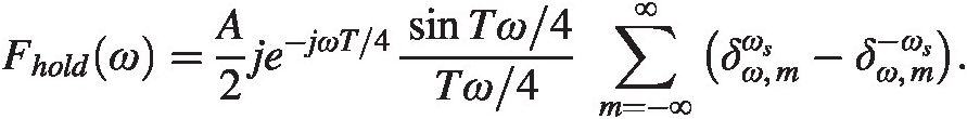
7. How does sampling conversion depend on duty cycle of the sampling clock? We have calculated the case where the hold width is the same as the sampling period in section “Voltage Sampling Theory.” Derive the more general case where the signal is held for some portion of the sampling period. The rest of the time output of the switch is zero.
8. Modern simulators have the ability to model nonlinear phenomena where a small signal gets up- or down-converted due to some nonlinear effect. This is often referred to as periodic ac simulation. We can use the model we have built in the voltage sampling section (“Voltage Sampling Theory”) to explore this effect analytically, by using the nonideal switch but replacing the noisy resistor with a signal source with a single frequency ωsωs and using the track and hold model. First, simplify by only looking at the first harmonic of the sample frequency and investigate how the signal source tone gets up-converted around this harmonic.


7.8 References
 Findit@CUHK Library | Google Scholar
 Findit@CUHK Library | Google Scholar
 Findit@CUHK Library | Google Scholar
 Findit@CUHK Library | Google Scholar
 Findit@CUHK Library | Google Scholar
 Findit@CUHK Library | Google Scholar
 Findit@CUHK Library | Google Scholar
 Findit@CUHK Library | Google Scholar
 Findit@CUHK Library | Google Scholar
 Findit@CUHK Library | Google Scholar
 Findit@CUHK Library | Google Scholar
 Findit@CUHK Library | Google Scholar
 Findit@CUHK Library | Google Scholar
 Findit@CUHK Library | Google Scholar
 Findit@CUHK Library | Google Scholar
 Findit@CUHK Library | Google Scholar
 Findit@CUHK Library | Google Scholar
 Findit@CUHK Library | Google Scholar
 Findit@CUHK Library | Google Scholar
 Findit@CUHK Library | Google Scholar