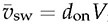
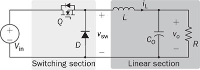
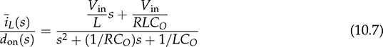
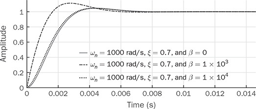
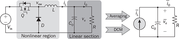
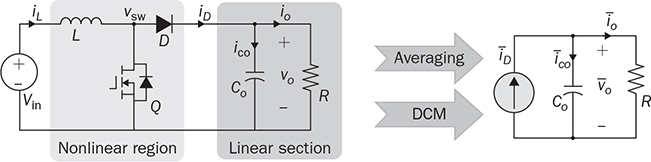
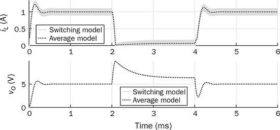
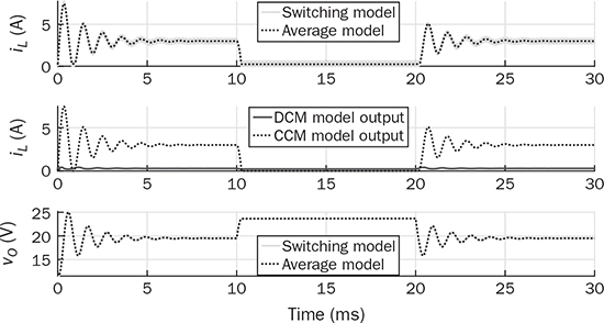
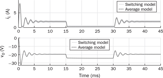
The trend of power converters leads to the utilization of high-frequency switching and shows nonlinear characteristics due to the on/off operation. When a power supply system, e.g., microgrid, is formed by significant numbers of switching-mode converters, simulation can be challenging, especially for long-term study of daily power generation from PV and wind, slow variation of the state of charge in the energy storage system (ESS), etc. The high switching frequency demands very high sampling rate in the simulation setting to maintain high switching resolution, which eventually results in slow simulation speed. Both academy and industry demand an efficient and generalized simulation model to evaluate long-term system operation of distributed renewable power generation and energy storage. Modeling and simulation are increasingly important for dynamic analysis and controller synthesis. Modeling is a general term that constructs mathematical models for the simulation study, dynamic analysis, or both. The averaging technique has been widely applied for modeling power converters since the low-frequency component critically dominates system dynamics. Thus, the averaging technique can neglect high-frequency switching effects but reveal key system dynamics for simulation and analysis. This chapter focuses on the averaging technique for numerical simulation and dynamic analysis. The method should support fast simulation without losing any critical dynamics in transient states. The modeling approach is based on the mathematical representation of system dynamics rather than any specific simulation tool. The approach is generalized for the whole operating status, including light load conditions and the DCM of power converters. The design and operation of high-efficiency power converters are mainly based on the fast on/off switching technology to manage and regulate power flow. High switching frequency, up to megahertz, becomes desirable, since the size and capacity of passive components, e.g., inductors and capacitors, can be significantly reduced to improve power density, reduce costs, and enhance system dynamics. For numerical simulation, the high switching frequency generally leads to slow numerical simulation to capture the fast switching dynamics. The sampling frequency for simulating switching-mode converters in discrete time is usually sized to be at least 100 times the switching frequency for accurate representation. For example, the sampling time should be 100 ns, assigned for simulation if a converter switching frequency is 100 kHz, which results in the 1% resolution of the switching duty ratio. When the sampling time is reduced to 10 ns, the resolution of the PWM is improved to 0.1%, which is more accurate and representative, but takes a longer time to fulfill the simulation. The majority focuses on special hardware and software to meet the demand for intensive simulation. However, the solution is very costly but is not general enough for wide implementation. The widely used simulation platforms have been listed in Sec. 1.4.2. The dynamics of high-frequency switching can be of interest for short-term analysis to reveal the dynamics in each switching cycle, which has been widely used in the steady-state analysis of inductor current and capacitor voltage for DC/DC conversion. However, the periodic oscillation effect is mostly unimportant for long-term analysis and simulation. The averaging technique for power electronics has been developed since the 1970s to analyze system dynamics. The averaging approach is based on the fact that the switching frequency is much higher than the critical dynamics that are commonly represented by LCR circuits. In CCM, the dynamics of both inductor current and capacitor voltage are as considered in the discussions that follow regarding the dynamic modeling and analysis. A standard buck converter can be divided into two regions, namely, switching and linear, as illustrated in Fig. 10.1. The linear section is formed by the passive components of L, CO, and R, which can be modeled by the circuit theory. The switching mechanism is formed by the semiconductors, switched for the power modulation and voltage conversion. The interlink between the linear region and nonlinear section is the voltage at the switching node, vsw, which is pulsating and discontinuous. The averaging computation focuses on the pulsating voltage, vsw, in which the averaged value is derived to be FIGURE 10.1 Buck converter for modeling by averaging based in CCM. FIGURE 10.2 Equivalent circuit of buck converter for modeling by averaging. where Besides the state-space representation, the system dynamics can be represented by the single-input-single-output (SISO) system using differential equations. When the averaged value of the output voltage is the controlling target, a differential equation can be derived from the two first-order equations in (10.1) and (10.2) into the second-order format of When the averaged value of iL is of interest, the differential equation can be derived to represent the SISO dynamic relation between the averaged current, ¯iL, and the on-state duty ratio, don, as The differential equations in (10.4) and (10.5) can be transferred to the frequency-domain representation using Laplace transform. The transfer function in s-domain is a typical way to show the dynamic correspondence of a SISO system. For the buck converter, the transfer functions become as in (10.6) and (10.7) with the consideration of the controlled outputs, where The DC gains in the generalized transfer functions are symbolized as K0v and K0i that represent the ratios between the outputs and inputs in the steady state. The denominator of Gi(s) is the same as that of Gv(s), which indicates two important parameters: the system damping ratio, ξ, and undamped natural frequency, ωn. The transfer functions show the difference in the numerators by comparing (10.8) with (10.9). The dynamic model of buck converters in the CCM has been derived by the averaging technique as a standard second-order transfer function, as in (10.8). The mathematical model indicates two poles without zero. The poles can be determined and demonstrated on a complex s-plane or pole-zero map. It is well known by the control theory that all poles must be in the left-half plane (LHP) to ensure a system stability. It should generally not be concerned since the dynamic model of a buck converter always shows the stability. Thus, the study should focus on the dynamic features regarding the values of the undamped natural frequency, ωn, and damping ratio, ξ. The important measure includes the settling time and percentage of overshoot in response to a step change. The undamped oscillation scenario in buck converters commonly refers to the non-load condition where R = ∞. The dynamic analysis indicates that non-load condition leads to the zero value of the damping factor, ξ = 0, according to (10.10). The analysis is based on the assumption that the Equivalent Series Resistance (ESR) in the circuit is zero. The switching operation triggers endless oscillation of the LC circuit and follows the resonant frequency of ωn. When 0 < R < ∞, the nonzero value of ξ indicates a damping effect in the circuit, which makes the self-oscillation disappear in the steady state. The value of ωn becomes the representative of the system dynamic speed. A fast response can be expected for the high value of ωn. According to (10.10), the high speed results from the low values of L × CO. The value of ξ represents how much damping or oscillation the system presents. According to (10.10), the damping factor for the buck converter depends on the parameters of the passive components, L, CO, and R. When the CCM is operated, a low value of R indicates light damping. The ratio of L and CO is also critical and related to the damping ratio, which should be considered in the design stage. Thus, a converter circuit design should be comprehensive to consider not only the steady-state ripples but also the dynamic performance regarding the response speed and damping factor. However, an over-damped system design should be avoided, e.g., ξ > 2, since it shows a sluggish dynamic response. Figure 10.3 demonstrates the effect of ωn and ξ on the step response regarding the response speed and damping performance, where Vin = 1. FIGURE 10.3 Step response of the second-order system showing effect of (a) ξ; (b) ωn. Significant oscillation and overshoot are visible in Fig. 10.3a when ξ < 0.3, which prolongs the settling time. The response speed is fast when ωn is high in the system dynamics, as demonstrated in Fig. 10.3b. The settling time of a step response regarding the system dynamics as in (10.8) can be estimated to be TABLE 10.1 Percentage of Overshoot in Step Response of Standard Second-Order Systems When the inductor current in a buck converter is the controlled objective, the dynamic analysis follows the transfer function in (10.9), where R = 1. It shows the same denominator as the transfer function in (10.8) with the same values of ωn and ξ. The difference lies in that the numerator in (10.9) presents a dynamic term of βis + 1, which indicates a zero with the value of FIGURE 10.4 Step response of second-order system with one minimal-phase zero, The boost converter shows the separation of the inductor, L, and the output capacitor, CO, as illustrated in Fig. 3.22a. Different from the buck converter, a linear region is no longer clearly distinguishable. When the active switch is on-state, the system dynamics has been derived and expressed in (3.32) and (3.33). When it is off-state, the differential equation is derived as (3.34) and (3.35) to illustrate the switching dynamics. The system dynamics should be identified by the state variables of iL and vo, which link to the energy storage components, L and CO. The control variable is the on-state duty cycle of don or the off-state duty ratio of doff for the PWM to switch the active switch, Q. In CCM, the state equations of (3.32) and (3.34) can be averaged within one switching cycle, TSW, and expressed as (10.11). Averaging the state equations of (3.33) and (3.35) in one switching cycle, TSW, leads to (10.12) in CCM. The variables of where Both (10.11) and (10.13) appear to be nonlinear due to the multiplication of FIGURE 10.5 Averaged model for simulating boost converters based on CCM. When a simulation model is developed, verification is important to prove its effectiveness. In this case, the output of the mathematical model is compared with the simulation result using the full-scale switching model, which has been developed and shown in Fig. 3.27. Based on the case study that developed in Sec. 3.4.5 and modeled in Sec. 3.4.6, the simulation comparison is illustrated in Fig. 10.6. It simulates the starting stage when the nominal duty ratio is applied to the PWM and leads iL and vo to rise and stabilize to the steady-state level. The output of the averaging model shows no information about the switching ripples but captures the critical dynamics in the step response. The averaging model is nonlinear but can be used for fast simulation when the CCM is guaranteed. The simulation can be much faster than the switching-based model since the details of switching dynamics are neglected. FIGURE 10.6 Simulation results to compare switching model and averaged model for boost converter. The buck-boost converter shows the separation of the inductor, L, and the output capacitor, CO, as illustrated in Fig. 3.37. When the active switch is on-state, the equivalent circuit is illustrated in Fig. 3.38a and the system dynamics are expressed by (3.52). When it is off-state, the equivalent circuit is plotted in Fig. 3.38b and the system dynamics are expressed by (3.53). In the CCM, the state equations in (3.52) and (3.53) can be averaged according to one switching cycle, TSW, and expressed as (10.11) and (10.12). The variables of Both (10.14) and (10.15) are nonlinear equations due to the multiplication of doff FIGURE 10.7 Averaged model for simulating buck-boost converters in CCM. For model verification, the output of the mathematical model is compared with the simulation result using the full-scale switching model, which has been developed and shown in Fig. 3.43. Based on the case study carried out in Sec. 3.6.5 and modeled in Sec. 3.6.6, the simulation comparison is illustrated in Fig. 10.8. It simulates the starting stage when the nominal duty ratio is applied to produce PWM output and lead the voltage and current to reach the steady state. The time-domain simulation indicates the agreement between the averaged model and the common switching model. The output of the averaging model shows no detail about the switching ripples but captures the critical dynamics in the step response. Both reveal the saturation time of iL and lead to the DCM during the transient stage due to the diode effect. FIGURE 10.8 Simulation results to compare switching model and averaged model for buck-boost converter. The averaging technique discussed in the last section is mainly based on the CCM, which is useful for fast simulation. In many applications, the discontinuous conduction mode (DCM) in steady state cannot be avoided since the power level depends on load condition. One example is the battery charger, where the power level can be low enough for the DCM when the battery is close to the full level of its state of charge. Further, the case study of the buck-boost converter enters the DCM during the transient stage even though the topology is designed and operated for the CCM, as illustrated in Fig. 10.8. A generalized approach is required to promote the fast simulation of the averaged models, which can represent the complete operating condition and cover critical dynamics and accurate steady state in both the CCM and DCM. The DCM happens when a converter uses diodes for the flywheeling purpose. It shows that the inductor current is low in the averaged value in comparison with its ripple magnitude, which has been addressed in Chap. 3. The inductor does not show sufficient energy storage capability in the circuit since the stored energy is always reset to zero for a certain time in each switching cycle. Therefore, the dynamics of the inductor current should be separately considered due to its discontinuity in the DCM. The DCM operation of a buck converter is discussed in Sec. 3.3.3 and illustrated in Fig. 3.10. Due to the discontinuity of iL, the dynamics of the averaged value cannot be considered a state variable in the linear representation, which is different from the CCM case. In DCM, the equivalent circuit is shown in Fig. 10.9, where the inductor is classified in the nonlinear region with the switching mechanism. The averaged value of the inductor current is modeled as a DC current source, where FIGURE 10.9 Buck converter for modeling by averaging based on DCM. For a full-time DCM operation, the simulation model can be built by Simulink to compute the averaged value of the inductor current ( FIGURE 10.10 Simulation model of buck converter for average current representation in DCM. The DCM of a boost converter is discussed in Sec. 3.4.4 and shown in Fig. 3.26. Due to the discontinuity of iL, the average value of iL can be computed by (10.20), where TSW refers to the switching cycle and other variables discussed below to follow the definition in Fig. 3.22. The equivalent circuit is demonstrated in Fig. 10.11 to model the boost converter in the DCM. The averaged value of the diode current, FIGURE 10.11 Equivalent circuit of boost converter for average current representation in DCM. where Following (10.20)–(10.24), the Simulink model can be built to determine the averaged values of the inductor current ( FIGURE 10.12 Simulation model of boost converters for average current representation in DCM. The DCM of a buck-boost converter has been discussed in Sec. 3.6.4 and illustrated in Fig. 3.42. Due to the discontinuity of iL, the same dynamic representation for the CCM cannot be applied to represent the nonlinear feature of current saturation. The equivalent circuit is demonstrated in Fig. 10.13 for the buck-boost converter in the DCM. The averaged value of the diode current, FIGURE 10.13 Equivalent circuit of buck-boost converter for modeling based on DCM. Following (10.25)–(10.29), the Simulink model can be built to represent the averaged values of the inductor current ( FIGURE 10.14 Simulation model of buck-boost converter for average current representation in DCM. In the previous sections, we discussed the averaged models separately for the CCM and DCM. The independent models could not cover the operational transition between the CCM and DCM due to load variation. This section focuses on a universal model to cover both operating modes in case of load variation and maintain fast simulation. In the CCM of a buck converter, the averaged value of iL is determined by the integration function expressed in (10.30). In a steady state, the DC offset is correctly maintained to present the continuous current flow since donVin = However, the value produced by the DCM model in (10.16) is accurate to represent the DCM and remains nonzero. Thus, the averaged value of the inductor current can be determined from the higher value resulting from either (10.30) and (10.16). The selection mechanism becomes universal regardless of the model difference between CCM and DCM. A generalized simulation model is developed including the selection mechanism and constructed by Simulink, as shown in Fig. 10.15. The inputs of the simulation model include don and Vin, and outputs real-time values of FIGURE 10.15 Complete simulation model of buck converters using averaging technique for both CCM and DCM. The performance of the developed model is verified by comparing the results with the common switching model, which has been established in Sec. 3.3.6 and shown in Fig. 3.15. The case study follows the same specification introduced in Sec. 3.3.5 and specified in Table 3.2. The comparison is illustrated in Fig. 10.16, covering the transition between the CCM and DCM. A sudden load variation from R = 5 Ω to R = 100 Ω leads to the transition from the CCM to DCM at the moment of 2 ms. Without changing the switching duty ratio, the output voltage variation is recognized, which is 5 V for the CCM and 6.36 V for the DCM in steady states. The simulation also shows that the load variation at 4 ms brings the operation back to the CCM, where the output voltage is 5 V in the steady state. The waveform agreement verifies the effectiveness of the averaged model to represent the full-scale operation of buck converters, regardless of load variation. The averaged model is 10 times faster than the conventional switching model for the same case study, captures the critical dynamics during the transit, and neglects high-frequency switching ripples. FIGURE 10.16 Simulation of switching between CCM and DCM due to load variation of buck converter. The same analysis can be applied to model boost converters; the correct estimation of ¯iL is selected from the averaged models of the CCM and DCM. The accurate representation is from the higher value of FIGURE 10.17 Complete simulation model using averaging technique for both CCM and DCM of boost converters. The universal model shows an integration of the CCM mathematical model, as illustrated in Fig. 10.5, and the DCM model, as shown in Fig. 10.12. The computations for the CCM and DCM are in parallel to produce the averaged values of the inductor current and diode current. The higher value of the estimated The evaluation is based on the performance comparison between the proposed averaging model with a conventional switching model, which has been established and shown in Fig. 3.27. The case study follows the same as the description in Sec. 3.4.5 and modeled in Sec. 3.4.6. The simulation result comparison is illustrated in Fig. 10.18. A sudden load variation from R = 10.56 Ω to R = 200 Ω leads to the transition from the CCM to DCM at the moment of 10 ms. Without changing the switching duty ratio, the output voltage variation is recognizable in Fig. 10.18, which is 19.5 V for the CCM and 23.7 V for the DCM. The load variation at 20 ms brings the operation back to the CCM and changes to the nominal load condition. The CCM and DCM models output the current values, of which the higher value is selected to be the correct variable, as indicated in Fig. 10.17. Figure 10.18 shows the waveform agreement and verifies the effectiveness of the universally averaged model for simulating boost converters. FIGURE 10.18 Simulation of switching between CCM and DCM due to load variation. Similar to the development for the boost converter, the averaged simulation model of buck-boost converters can be derived to cover the operation of the CCM and DCM. The selection mechanism can be identified to pick the higher value of FIGURE 10.19 Complete simulation model of buck-boost converters using averaging technique for both CCM and DCM. FIGURE 10.20 Simulation of switching between CCM and DCM due to load variation of buck-boost converter. The performance of the universal model is verified by comparing the results with the common switching model, which has been developed in Sec. 3.6.6 and shown in Fig. 3.43. The case study follows the same specifications introduced in Sec. 3.6.5 and specified in Table 3.4. The comparison is illustrated in Fig. 10.20 to test the transition between the operations of the CCM and DCM. The initial transient state shows a short DCM operation from 1 to 1.5 ms. A sudden load variation from R = 10.56 Ω to R = 200 Ω leads to the sudden transition from the CCM to DCM at the moment of 15 ms. Without changing the switching duty ratio, the output voltage variation is recognizable, which is changed from −19.5 V in the CCM to −24.3 V for the steady state of the DCM. The DCM of the inductor current is shown from 15 to 30 ms. The load resistance changes back to the nominal rating at 30 ms, which ends DCM and brings the operation back to CCM and the nominal operation. After the transient state, the output voltage is −19.5 V, agreeing with the specification. The waveform agreement verifies the effectiveness of the universally averaged model for simulating buck-boost converters. The averaged model captures the critical dynamics during the transit but neglects the details of high-frequency switching ripples. The averaged model allows a low sampling rate for simulation, which is significantly faster than the conventional switching model. This chapter focuses on the averaging technique to model DC/DC converters regarding the operation of the CCM and DCM. The critical system frequency mostly refers to the slow dynamics that drag the overall system response. For power converters, the critical dynamics are determined by the passive components with energy storage components, e.g., inductors and capacitors. They provide low-pass filtering to mitigate high-frequency ripples, but dominate the system dynamics. Modeling a buck converter in the CCM is straightforward because of the clear separation between the nonlinear and linear region. The averaging process leads to a second-order linear system that can be directly used for dynamic analysis, as described in Sec. 10.2.2. The dynamic characteristics are commonly considered an advantage of the buck topology. The linear model is based on the assumption that the parameters of passive components, e.g., L, C, and R, are constant during the modeling process. The modeling study also covers the boost and buck-boost converters that are operated in the CCM. However, the averaging process results in the mathematical models, which are nonlinear but useful for the simulation purpose. The DCM operation shows different dynamics from the CCM cases of buck, boost, and buck-boost converters. The inductor current cannot be considered one of the dynamic variables due to the discontinuity in the DCM. The system dynamics of the three converters become dominated by the circuit of the output capacitor and the load, an RC circuit. The value of the discontinuous inductor current is averaged and injected into the RC circuit to represent the system dynamics of the buck converter. In the case of boost and buck-boost converters, the diode current is averaged and injected into the RC circuit to represent the system dynamics. The regular switching models developed in Chap. 3 are typically restricted by the switching frequency and result in low simulation speed. The universal simulation models are presented in this chapter, which flexibly cover transitions between the CCM and DCM. The advantage of the averaged models lies in the allowance of large step size in numerical solvers to achieve high simulation speed. Even though the chapter demonstrates only three case studies, the same averaging technique is general and can be applied to the dynamic analysis and simulation of other topologies. 1. M. Evzelman and S. Ben-Yaakov, “Simulation of hybrid converters by average models,” IEEE Transactions on Industry Applications, Vol. 50, no. 2, pp. 1106–1113, March 2014. 2. W. Xiao, H. Wen, and H. H. Zeineldin, “Affine parameterization and anti-windup approaches for controlling DC-DC converters,” in Proc. IEEE International Symposium on Industrial Electronics, Hangzhou, 2012, pp. 154–159. 3. W. Xiao and P. Zhang, “Photovoltaic voltage regulation by affine parameterization,” International Journal of Green Energy, Vol. 10, no. 3, pp. 302–320, February 2013. 4. I. Syed, W. Xiao, and P. Zhang, “Modeling and affine parameterization for dual active bridge DC-DC converters,” Electric Power Components and Systems, Vol. 43, no. 6, pp. 665–673, March 2015. 5. S. Jiao and W. Xiao, “Fast simulation technique for photovoltaic power systems using Simulink,” in Proceedings of the International Future Energy Electronics Conference, Singapore, 2019. 10.1 Following the case study, build your own averaged models for the CCM operation of buck, boost, buck-boost, and Ćuk converters to compare the simulation performance with the outputs of high-resolution switching models. 10.2 Following the case study, build your own averaged models for the DCM operation of buck, boost, buck-boost, and Ćuk converters to compare the simulation performance with the outputs of large-scale switching models. 10.3 Combine the CCM and DCM and create the universal models for the buck, boost, buck-boost, and Ćuk converters. Verify the model by comparing the simulation result with the output of a conventional switching-based model.
CHAPTER 10

Averaging for Modeling and Simulation
10.1 Switching Dynamics
10.2 Continuous Conduction Mode
10.2.1 Buck Converter
 when non-ideal factors are neglected. The voltage conversion is based on the proportion of the on-state duty ratio, don, in CCM. After the averaging, the equivalent circuit can be plotted as shown in Fig. 10.2. The linear circuit analysis can be applied and expressed by


 and
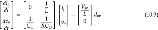
and  represent the averaged values of the inductor current and output voltage, respectively. The model can be transformed to the state-space format in (10.3), where the two states are represented by
  and
and  , while the input is the on-state duty ratio of the active switch, don. The state-space model represents a linear physical system when Vin is constant for the modeling. The model becomes available for the state-space-based analysis and controller design. The state feedback is a useful control technique to regulate the state variables,
  and
and  , and determine the control action, don.


 and
and  , respectively. The transfer functions in (10.6) and (10.7) are commonly represented by the generalized formats, as expressed in (10.8) and (10.9) for the following analysis.


10.2.2 Dynamic Analysis of Second-Order Systems
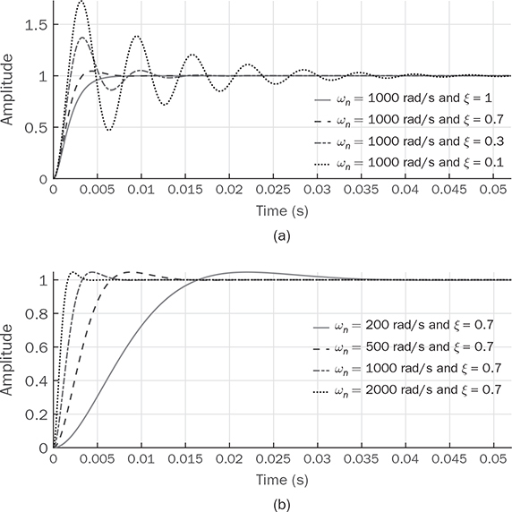
 for the standard second-order transfer function. Table 10.1 summarizes the value of the percentage of overshoot (P.O.) in step response of the transfer function in (10.8), which is influenced by the value of ξ. When ξ = 0.7, the step response shows the value of P.O. less than 5% and fast response speed, as shown in Fig. 10.3a. The information can be treated as a reference for dynamic analysis and control system design.

 . The negative value of the zero indicates a minimal-phase (MP) system. Figure 10.4 demonstrates the effect of minimal-phase zero during the step response. When the absolute value of
  is high, its effect is insignificant to the system response. If βi is high in value, such as βi = 10−3, the step response shows fast speed in the initial stage; however, it causes higher overshoot in comparison with the case of βi = 0 and βi = 10−4. Following (10.10), the βi value is affected by the design of CO and changed with the load condition, R. For buck converters, a high overshoot is expected in the step response of light load conditions since R is high in value.

10.2.3 Boost Converter
 represent the averaged values of vo, io, and iD in each switching cycle, respectively, which are defined as follows and as presented in Fig. 3.22a.


 and doff = 1 − don in the CCM. Thus, the differential equation in (10.12) becomes

 and
and  . The model can be used for simulation purpose or nonlinear control approach. Following the nonlinear questions of (10.11) and (10.13), a simulation model can be constructed and based on the averaged variables of
  and
and  , and
, and  . Figure 10.5 illustrates the Simulink model, which outputs the averaged value of iL and vo. The input includes the on-state duty ratio (don) and the averaged value of the output current, which can be determined by the load condition in response to the output voltage.
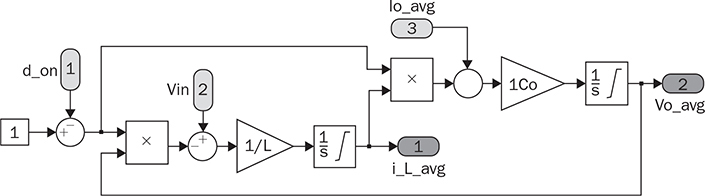
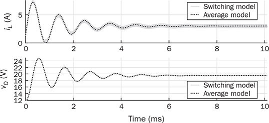
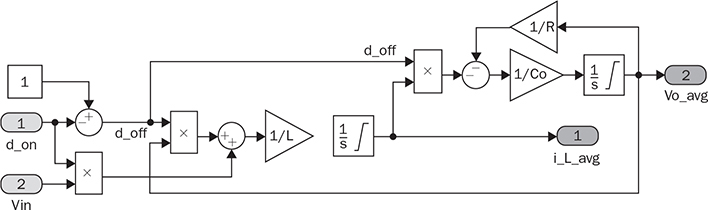
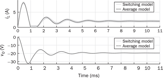
10.2.4 Buck-Boost Converter
 and
and  represent the averaged values of vo and iL, respectively, which are defined and shown in Fig. 3.37. In the CCM, the averaged value of the diode current is expressed by
  , where doff = 1 − don.

 and doff
 since all are variables. The nonlinear model can be directly used for simulation purposes. Following the formula of (10.14) and (10.15), a simulation model is constructed to represent the averaged variables of
  ,
,  , and
, and  with the duty ratio as the control input, as illustrated in Fig. 10.7. The input includes the on-state duty ratio (don) and the averaged value of the output current, which can be determined by the load condition in response to
  . The saturation should be applied to the integration block when the diode is used, which limits the polarity of the inductor current and capacitor voltage.
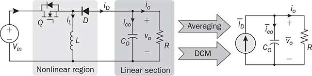
10.3 Discontinuous Conduction Mode
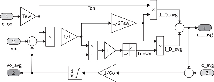
10.3.1 Buck Converter
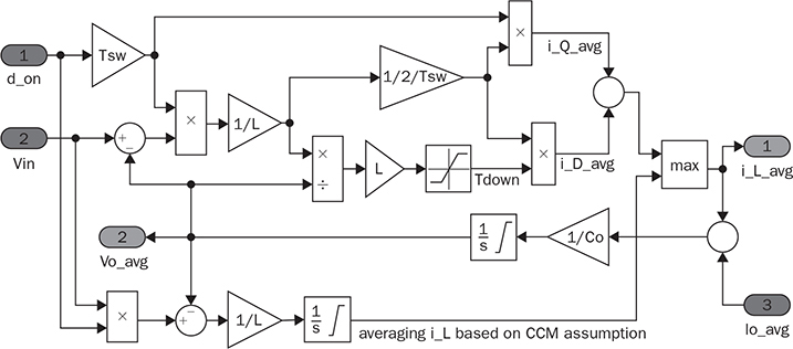
 , and applied to the circuit formed by CO and R. The average value of iL can be determined by (10.16) where TSW refers to the switching cycle and other variables follow the definition in Fig. 10.9 and Fig. 3.10.

 and
and  represent the averaged value of iQ and iD, respectively. The peak-to-peak ripple can be derived by (10.17); the TDOWN is determined by (10.18). The averaged value of the output voltage,
  , and its dynamics can be determined by the injected current,
 , into the circuit of CO and R, as illustrated in Fig. 10.9.


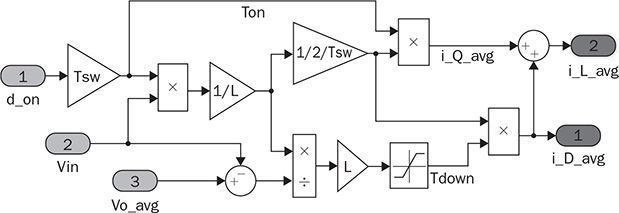
 ), as illustrated in Fig. 10.10. The model computes the peak-to-peak value of iL, the time period of down state, TDOWN, and then the averaged value,
  , by following (10.17), (10.18), and (10.16), respectively. The averaged value of the output voltage is derived by (10.19) and formulated in the averaging model.

10.3.2 Boost Converter
 , becomes the interlinking variable to represent the nonlinear section output and the input of the linear region.

 represents the averaged value of iQ and
  is the averaged value of iD. The peak-to-peak ripple can be derived by (10.21), the TDOWN is determined by (10.22), and the average values of iQ and iD are expressed by (10.23) and (10.24), respectively. The averaged value of the output voltage,
  , can be determined by the injected current,
  , and the CR circuit, as illustrated in Fig. 10.11.


 ) and diode current (
 ) in DCM, as shown in Fig. 10.12. The averaged value of diode current,
  , is injected into the RC circuit at the output terminal and leads to the variation of the averaged voltage,
  .
.
10.3.3 Buck-Boost Converter
 , becomes the variable to represent the nonlinear section output, which is negative in value. The peak-to-peak ripple of iL can be determined by (10.25), where TON = donTSW. The decreasing time period of iL results from (10.26) where
  < 0. According to energy balancing, the averaged value of iD is expressed by (10.27) when the conversion loss is ignored. The averaged value iQ can be determined by (10.28). The averaged value of iL is expressed by (10.29). The averaged value of the output voltage,
  , can be determined by the injected current,
  , and the RC circuit, as illustrated in Fig. 10.13.


 ) and diode current (
 ) in the DCM, as shown in Fig. 10.14. The value of
  is determined by the model in real time and applied to the circuit of R and CO to simulate the averaged value of the output voltage.
10.4 Integrated Simulation Model
10.4.1 Buck Converter
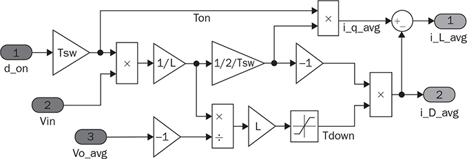
 . When the operation enters the DCM of a buck converter, the inductor current is reset to zero and presents discontinuity at every switching cycle. The value of
  is higher than that of donVin in the DCM, which makes donVin −
  < 0. The continuous integration of the CCM model in (10.30) leads to zero value of
  , which is incorrect in the DCM.

 and
and  .
.
10.4.2 Boost Converter
 , resulting from the CCM- and DCM-based models. In the DCM, the averaged value of
  estimated by (10.11) is reset to zero, which is incorrect. Thus, the averaged value of the inductor current can be selected from the higher value resulting from either (10.11) and (10.20), which covers both the CCM and DCM. A generalized simulation model can be formulated by the selection mechanism and constructed by Simulink, as shown in Fig. 10.17.
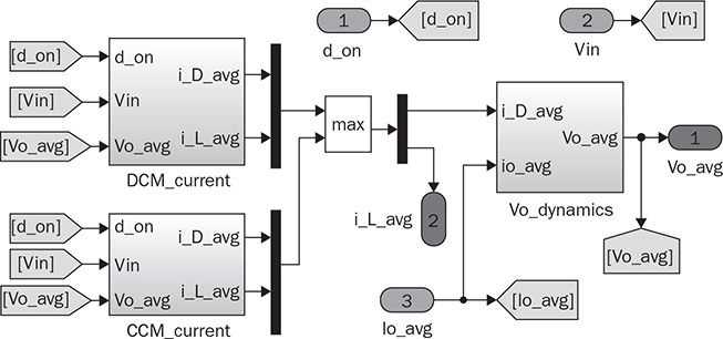
 is selected as the correct input to the RC circuit for determining
  , as shown in Fig. 10.17. The model takes the inputs of the input voltage and the on-state duty ratio as the control input. The load condition can be independently implemented to represent the value of ¯io corresponding to the variation of
  .
.
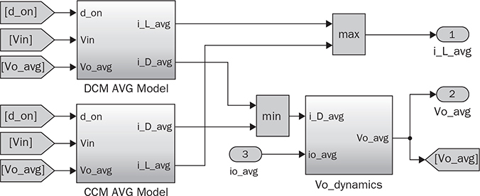
10.4.3 Buck-Boost Converter
 from the two model outputs representing the CCM and DCM operation, as illustrated in Fig. 10.19. According to the current definition in the buck-boost converter, the diode current is negative in value. The correct value of
  is selected and injected into the RC circuit, which affects the variation of the output voltage,
  . Figure 10.19 shows the averaging models of the CCM and DCM, which have been developed earlier and shown in Figs. 10.7 and 10.14, respectively.
10.5 Summary
Bibliography
Problems