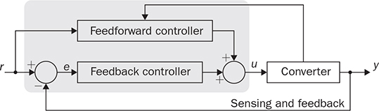
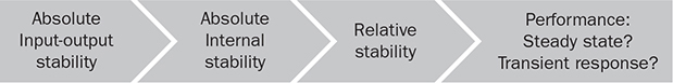
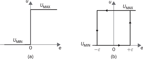
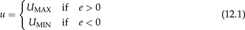
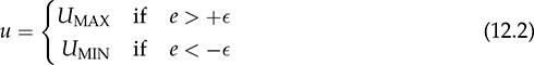
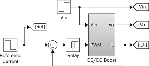
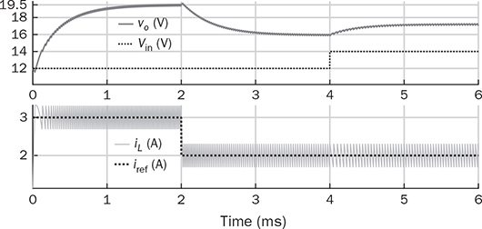
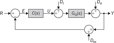
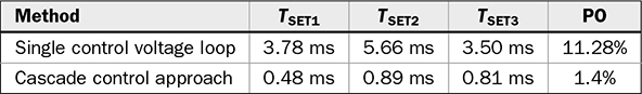
Control engineering is an important subject within power electronics, as discussed earlier in Sec. 1.2. Power conversion cannot be properly operated without control and regulation of the level of voltage, current, or power. A typical two-degreeof-freedom (2DOF) control diagram for power electronics is demonstrated in Fig. 12.1. The desired output is indicated as r, which is also called the reference or set point. The output variable is symbolized as y, which is expected to follow the value of r. In power electronics, r and y commonly refer to the values of voltage, current, or power. The difference between the desired and the actual value is called the error, calculated by e = r − y. The control action is represented as u, which usually refers to either switching duty ratio or phase shift angle. When u is properly applied, the control objective of y = r can be achieved in steady states. FIGURE 12.1 Typical control configuration for power converters. The feedforward controller (FFC), shown in Fig. 12.1, is an effective way to improve the performance in terms of reference following and disturbance rejection. The direct format of FFC is simple for stability analysis. The concept can be easily understood by an example. In the CCM, the voltage conversion ratio of a buck converter is theoretically proportional to the applied duty ratio of pulse width modulation (PWM). When the voltage levels of the input and the expected output are known or predictable, the control variable of the duty ratio can be directly determined and used as the straightforward form of the FFC. The configuration can save the significant correction effort through the feedback control loop and shorten the settling time to reach the steady state. The FFC is typically designed by the well-known system information between the control action and system response. The feedback controller (FBC) has been widely utilized and forms the closed control loop, which includes sensing, feedback, and correction, as shown in Fig. 12.1. The real-time correction is capable of maintaining the desired output and mitigating non-ideal factors regarding disturbance and model uncertainty. Thus, the FBC is considered as the mainstream in controlling power conversion to reach the desired performance. The FFC becomes an additional function to coordinate more variables into the control system, and therefore improves the performance. In this chapter, the linear control theory is studied and applied to design and operates power converters to meet the system requirement. A control system should be evaluated and based on the following specifications: • Absolute stability between input and output is the fundamental requirement for control engineering. It is defined that the system output should always be bounded if the input is bounded. It is referred to the general stability definition in terms of the bounded input and bounded output (BIBO). • Internal stability should be guaranteed that all signals inside the control system are always bounded. • System robustness should be guaranteed, which refers to the relative stability. It measures the distance from the boundary of instability. Highly robust systems can effectively prevent from any instability caused by unpredictable factors, such as model uncertainty, noise, disturbance, time variance, and temperature effect. • Ideal control performance indicates the zero value of steady-state error. • Fast response is generally required to demonstrate control performance in response to the setpoint change or against disturbance. The time from one steady state to another should be short. Meanwhile, the transient response is expected to be smooth, without significant deviation or oscillation. When a closed-loop control system is designed, it is important to follow the procedure to evaluate its stability, robustness, and performance, as recommended in Fig. 12.2. The absolute stability is critically required for all expected operating conditions. The control performance can only be improved with guaranteed sufficient relative stability or robustness. It is mostly a trade-off between the system’s robustness and the control performance. When the absolute instability is guaranteed, the controller can be iteratively tuned to reach the optimal balance between the system robustness and performance. FIGURE 12.2 Evaluation procedure of closed-loop control systems. The on/off switching is widely used in power electronics to modulate and/or regulate power flow in terms of voltage and current. The switching concept is simple but can be directly utilized for control and regulation. It follows the feedback control mechanism to achieve the function of error detection and correction, and forces the output, y, to follow the setpoint, r. The mechanism follows the simple idea of “true or false” or the boolean logic of “1 or 0.” A simple on/off control scheme is shown in Fig. 12.3a, which can be mathematically described by FIGURE 12.3 Demonstration of on/off control: (a) ideal concept; (b) hysteresis. where UMAX leads to the increase in y to be close to r if r > y; meanwhile, UMIN results in the decrease in y if y > r. The on/off operation eventually keeps the output, y, close to the setpoint and e ≈ 0. In power converters, the UMAX can be referred to as turning on an active switch, which leads to an increase in inductor current. On the contrary, the action of UMIN is the extreme action of turning off the active switch and causing a decrease in the current. The on/off controller directly produces switching signals to drive active switches, which can neglect the dedicated PWM mechanism. The operation is demonstrated in Fig. 12.3a, which aims to correct the difference between y and r and forces e ≈ 0. However, the control implementation is sensitive to noise, which can make u switch randomly between UMAX and UMIN at an uncontrollably high frequency. Therefore, the on/off control introduces a hysteresis band or tolerance to improve its robustness against noise. The hysteresis controller is often called the bang-bang controller, which is expressed in (12.2) and illustrated in Fig. 12.3b. The approach adds tolerance to avoid extremely frequent transitions between UMAX and UMIN but sacrifices the steady-state performance. When the error, e, is within the range between −ε and +ε, the controller maintains its current output, unchanged, until the condition for the alternative state is satisfied. Thus, the output, y, is controlled to oscillate around the reference signal within the hysteresis band of ±ε. The assigned value of ε shows the trade-off between the steady-state error and the on/off switching frequency. It is known that all physical components show switching speed limit; meanwhile, the high-frequency switching commonly results in power loss, as discussed previously. The hysteresis controller follows a nonlinear approach to form the feedback control loop. The design is simple, because mathematical modeling is unnecessary. It has been widely used in power converters to regulate inductor current. The case study is based on the boost converter, the parameters of which have been specified in Sec. 3.4.5. The steady-state analysis shows that the inductor current increases when the active switch is on. Otherwise, the inductor current of the boost converter decreases. A simulation model is constructed to demonstrate the control operation to regulate the inductor current, as shown in Fig. 12.4. A hysteresis controller is constructed by Simulink using the “Relay” block. The output for the “Relay” block switches between two specified values, “0” and “1,” which can control power switching. The hysteresis band (±ε) can be programmed inside the block. The inductor current is fed back for the hysteresis controller for regulation. The inductor current is expected to follow the reference signal indicated in the Simulink diagram. The assigned value of ε is 0.3 A, which is specified in the “Relay” block for the hysteresis control operation. The simulation result is illustrated in Fig. 12.5. FIGURE 12.4 Simulation model for hysteresis control to regulate inductor current of a boost converter. FIGURE 12.5 Simulation result for hysteresis control to regulate inductor current of a boost converter. The converter is controlled for the inductor current to be 3 A at the start, which represents the nominal condition. At the moment of 2.5 ms, the current reference is changed to 2 A. At the moment of 5 ms, a disturbance is introduced by a step change of the input voltage (Vin) from 12 to 14 V, as indicated in Fig. 12.5. The hysteresis controller proves its effectiveness and maintains the inductor current, iL, to follow the command signal, iref, changing from 3 to 2 A. The peak-to-peak ripple of iL is 0.6 A, which agrees with the converter specifications presented in Table 3.3. The switching frequency can be measured as 50 kHz to follow the current ripple rating at the nominal condition. The inductor current variation leads to the change in the output voltage, vo, since the load resistance is constant. When the output voltage is treated as the controlled variant, the inductor current regulation becomes the inner feedback loop. The cascade approach can be implemented to reach the voltage regulation, which will be discussed in Sec. 12.5. Affine parameterization is a controller design technique, which is based on mathematical modeling and dynamic analysis. The method makes controller design straightforward and guarantees the internal stability and control performance when the system modeling is properly performed. It is sometimes called the Youla parameterization and Q design. For a SISO system, the design procedure is as demonstrated in Fig. 12.6, where R is the reference and Y symbolizes the controlled variable. FIGURE 12.6 Concept of affine parameterization for design and implementation. During the design stage, the transfer function of Q(s) is introduced for the open-loop system analysis. For the series formation, as expressed in (12.3), the absolute and internal stability can be guaranteed when the transfer functions of Q(s) and G(s) show the feature of BIBO. The series form of Q(s)G(s) is straightforward for stability analysis, but shows no correction mechanism. For practical implementation, the control performance cannot be guaranteed if Y is deviated from R due to unpredictable disturbance or non-ideal factors. Thus, the mainstream of control configuration is based on the negative feedback mechanism. The same formation of Q(s)G(s) can be equivalently transferred to the closed-loop format that includes the correction function and the feedback controller, C(s), as illustrated in Fig. 12.6. The closed-loop implementation indicates the correction mechanism that any error between the reference, R, and the plant output, Y, can be detected and corrected by the controller. The transfer function of the closed-loop system demonstrates a rational form. The individual stability of the transfer functions of C(s) and G(s) cannot indicate the internal stability of the closed-loop showing the relation between Y and R. Therefore, the design stage starts from the synthesis of Q(s)G(s) to guarantee system stability. The equivalence between the transfer functions in (12.3) and (12.4) leads to the feedback controller that can be synthesized by (12.5). Following affine parameterization, the internal stability of the closed-loop system can be guaranteed. The controller synthesis simply takes advantage of both the open-loop stability analysis and closed-loop control implementation. Through the modeling process introduced in Chaps. 10 and 11, the mathematical model, G0(s), should be available to represent the dynamics of power converters in either the large-scale or small signals. The transfer function, G0(s), should be verified by either simulation or experiment before the controller synthesis is proceeded. Figure 12.7 illustrates the recommended design procedure using affine parameterization. The desired closed-loop transfer function, FIGURE 12.7 Design procedure of affine parameterization. The transfer function of the feedback controller is then derived by (12.5). The relative stability or robustness should be evaluated by analyzing the transfer function of C(s)G0(s) regarding the phase margin, gain margin, and sensitivity peak. When the robustness is satisfied, the feedback controller is ready for the closed-loop implementation. When a converter model is derived and verified, the relative degree of G0(s) can be determined, which shows the difference between the number of poles (Npole) and the number of minimal-phase (MP) zeros, Nzero. The relative degree is computed by Npole − Nzero, which is generally zero for a physical system. Based on the dynamic modeling in Chaps. 10 and 11, the converter models can be summarized into four types, which are expressed from (12.7) to (12.10). G0(s) is generally symbolized to represent a group of converter models for the following synthesis regardless of the difference in types and parameters. The relative degree of (12.7) and (12.9) is 1, where βi > 0. The transfer function in (12.8) shows the relative degree of 2. The model in (12.10) shows a non-minimalphase (NMP) zero since βv > 0. Following G0(s), the next step is to specify the desired closed-loop transfer function, FQ(s), according to the design procedure, as shown in Fig. 12.7. The step is critical with the consideration of the trade-off between the closed-loop performance and stability. The first-order transfer function, as expressed in (12.7), has been developed to represent the dynamics for the dual active bridge (DAB). Meanwhile, the converters of buck, boost, and buck-boost also show the first-order dynamics when the DCM is considered, which are discussed in Sec. 11.4. The FQ(s) should be defined as a first-order transfer function expressed in (12.11) to match the relative degree. The transfer function in (12.9) represents another group when the inductor current is the controlled target, which includes the topologies of buck, boost, and buck-boost. Such transfer functions are shown in (10.9), (11.29), and (11.42), which also indicate the relative degree of 1. The FQ(s) should be defined the same way as in (12.11) to match the relative degree. The DC gain of FQ(s) is 1, indicating the zero steady-state error. The speed of dynamic response is specified by the value of αcl in (12.11). The settling time of the step response can be estimated to be 4αcl, which is used to determine the value of αcl. A converter’s model can show the relative degree of 2, which is represented by (12.8). This model has been developed in Sec. 10.2.1 for the buck converter in the continuous conduction mode (CCM). The desired closed-loop function for such systems should be specified by (12.12), which can also be converted into (12.13) where The NMP system has been modeled in (11.27) and (11.40) regarding the dynamics of boost and buck-boost converters. The general form is shown in (12.10) for the following analysis. Figure 12.7 shows that the development of Q(s) requires the inverse transfer function, G0(s)−1. However, the inverse transfer function of the NMP G0(s) results in a right-hand-plane (RHP) poles that become unstable. To avoid any harmful zero-pole cancellation, the NMP zero should remain in FQ(s) according to affine parameterization. Thus, the transfer function for the closed-loop system should be specified as (12.14) or (12.15) to admit the existence of the NMP zero. The value of βv follows the same in (12.10). Due to the negative effect of the NMP zero, the closed-loop specification should be conservatively designed, which is required to maintain sufficient stability margin and robustness. For the first-order system shown in the expression of (12.7), the desired closed-loop transfer function in (12.11) is specified. The transfer function of Q(s) can be derived and expressed as in (12.16), which is considered to be stable and proper. Following (12.5), the function of Q(s) and G0(s) results in the transfer function of the feedback controller, C(s), as expressed in (12.17). The controller can be transferred to the standard format of a proportional-integral (PI) controller showing the proportional gain of Following the converter transfer functions in the format of (12.9), the desired closed-loop transfer function is also specified by (12.11) since the relative degree of G0(s) is 1. Following (12.6) and the converter transfer function, the Q(s) can be derived and expressed in (12.18). When the function Q(s) is verified for stability, the design process leads to the feedback controller transfer function, as expressed in (12.19). The transfer function can be converted into a proportional-integral-derivative (PID) controller, which will be discussed further in Sec. 12.4. When the relative degree of 2 is concerned, such as the converter transfer function for the output voltage of buck converters, the desired closed-loop system should be specified by (12.13). The transfer function of Q(s) can be derived into (12.20) according to the converter transfer function. When Q(s) is verified to be stable and proper, the design process can be continued by (12.5) into the feedback controller transfer function in (12.21). The transfer function of C(s) can also be converted into a PID format. When a NMP system is considered, the desired closed-loop system is specified by (12.15) to avoid any harmful pole-zero cancellation. The transfer function of Q(s) can be derived into (12.22) according to (12.6) and (12.10). After the Q(s) is verified to be stable and proper, the design process leads to the feedback controller transfer function that is the same as (12.21). In general, the Q(s) is an interlinking function that leads to the design of a feedback controller for the closed-loop implementation. Affine parameterization leads to the design of a closed-loop system with the absolute and internal stability. However, a real-world control system is coupled with non-ideal factors, such as disturbance and noise, as illustrated in Fig. 12.8. The indicators of Di, Do, and Dm represent the input disturbance, output disturbance, and measurement noise, respectively. For power converters, the inaccuracy of duty ratio or contaminated PWM signal results in the input disturbance. Any sudden or unpredictable load variation leads to the output disturbance, Do. It is known that all real-world signals cannot avoid noise coupling. Further, the power switching operation is nonlinear in nature. The mathematical models are based on the approximation techniques of averaging, linearization, and various levels of assumption. Model uncertainty is another concern. Therefore, the robustness in control system design should be of concern and analyzed. FIGURE 12.8 Illustration of real-world feedback control systems. When a feedback controller, C(s), is synthesized, one important measure is the relative stability of the closed-loop system. The relative stability indicates the system robustness and measures how far a nominally stable system enters endless oscillation or instability with the consideration of unpredictable disturbance, non-ideal environment, modeling inaccuracy, and model uncertainty. The common index for the measure includes the phase margin, gain margin, and sensitivity peak. The sensitivity function is defined by the linear control theory and expressed by (12.23). The function represents the transfer function between the output disturbance (Do) and the closed-loop output, Y, as indicated in Fig. 12.8. The So(s) also indicates how sensitive a closed-loop stability is affected by the model uncertainty. The sensitivity peak is the highest amplitude that happens at a certain frequency. It becomes an important measure of the system robustness, which is expected to be low to achieve high system robustness. Based on the derived transfer function, C(s)G0(s), the stability margins and sensitivity peak can be detected and evaluated. Either Bode diagrams or Nyquist plots can be applied for analyzing the relative stability. In MATLAB, the functions of “margin” and “nyquist” are commonly used for the Bode and Nyquist analyses, respectively. For demonstration only, a plant transfer function is shown as FIGURE 12.9 Bode plot of G(s)C(s) to illustrate phase margin and gain margin. The Nyquist plot is another way to illustrate the relative stability and robustness, as shown in Fig. 12.10 for the same case study. The critical point is shown as (−1, 0) in the complex graphical plot, where the gain is expressed by |C(s)G(s)| = 1 and the phase angle is indicated by Φ = −180°. Operating at the critical point results in endless system oscillation; therefore, it sets the boundary of the stable region of the system. The phase margin, Φm, is indicated in the Nyquist plot, which refers to the angle value, 32.5°. It is known that the more degrees of phase margin is, the better robustness of the closed-loop system possesses. As a rule of thumb, the phase margin should not be lower than 45°. The a shows the distance from the original point (0, 0) to the zero-crossing point. The value can be found as 0.40, which is the indicator of the gain margin since the gain margin in dB is expressed by FIGURE 12.10 Nyquist plot of G(s)C(s) to illustrate phase margin, gain margin, and sensitivity peak. One measure in Fig. 12.10 is shown as b, which shows the closest distance between the Nyquist curve and the critical point. The distance b is relative to the peak magnitude of the sensitivity function, which is expressed by (12.24). The peak happens at a certain frequency, which can be illustrated by the bode diagram of So(s), as shown in Fig. 12.11. The longer distance of b indicates decent system robustness since it represents the lower sensitivity peak. In this case study, it is shown as b = 0.41, which can be translated into max |So| = 2.44, as indicated by the Bode diagram in Fig. 12.11. A high sensitivity peak should be avoided in the closed-loop design. A good system robustness can be expected by b > 0.5 or max |So| < 2. FIGURE 12.11 Bode diagram to demonstrate the sensitivity function and the peak. In general, the relative stability that includes the phase margin, gain margin, and sensitivity peak measures the distance from the critical point, which is the boundary into system instability. The further the distance is, the better robustness can be achieved for the closed-loop control system. When the stability measure of phase margin, gain margin, or sensitivity peak cannot meet the specification, the controller can be retuned to meet the requirement. A common practice is to lower the DC gain of the controller function. The early case study shows that the controller FIGURE 12.12 Nyquist plot of G(s)C(s) to illustrate the effect of controller gain reduction. Feedback controllers can be implemented by either analog circuits or digital controllers. The trend is to use the digital microcontroller and field-programmable gate array (FPGA), which are flexible and powerful for the implementation of comprehensive and advanced control algorithms. A typical structure for the digital control system is shown in Fig. 12.13, in which the digital controller function, Cz, is included for the implementation. The modern micro-controller is powerful to be integrated with the functions of sampler, analog-to-digital converter (A/D or ADC), PWM generator, and holder. A limiter is indicated in the diagram that avoids the signal of u(k) out of the physical constraint. For example, the duty ratio of PWM should be within the range from 0 up to 100%. The holder and sampler serve as the interface between the continuous-time signal and the discrete-time signal. In the power train circuit, the transducer is required to measure the controlled variable, e.g., voltage or current. The signal conditioner is an analog circuit to calibrate the measured signal and make it robust and noise-free for signal transmission. FIGURE 12.13 Typical digital control structure for power electronics. A digital controller can be directly converted from the controller transfer functions in the s-domain, which are shown in (12.17), (12.19), and (12.21). The MATLAB function “c2d” supports the conversion from the s-domain to the z-domain. The sampling time of the control loop should be specified for the “c2d” conversion. The short sampling time generally leads to the closing performance between the analog controller and the digital alternative. A common practice is to adopt the sampling frequency the same or multiple times of the switching frequency since the frequency is much higher than the critical system dynamics. The setting automatically supports the operational synchronization between the control loop and the PWM operation. The transform method of “Tustin” is commonly used to be specified for the controller discretization. The “Tustin” transformation is based on the approximation of For programming, the control algorithm in (12.25) can be translated into a difference equation to update the controller output in discrete time, as expressed in (12.26). The variable u(k) can refer to the updated value of the duty ratio for PWM, as indicated in Fig. 12.13. The u(k − 1) and u(k − 2) are the historical values in the last two sampling cycles. The e(k) represents the latest error between the reference, r(k), and the feedback, y(k). The e(k − 1) and e(k − 2) are the recorded errors in the past two sampling cycles. Following the PI controller expressed in (12.17), the “Tustin” transformation leads to the controller transfer function into (12.27) in the z-domain. The control programming can follow the difference equation in (12.28) to update the controller output in every sampling cycle. High sampling frequency is desired since the digital control is akin to the operation in continuous time. However, the sampling frequency is sometimes limited by the computation capability of low-end microcontrollers. Furthermore, an unavoidable time delay is introduced in the control loop that resulted from the computation, A/D conversion, sampler, and holder. The time delay should be considered in the stability analysis since it might significantly reduce the stability margins and even lead to instability. Affine parameterization, introduced in Sec. 12.3, does not take the time delay of the digital control loop into consideration. The time delay level depends on the sampling frequency, speed of digital controllers, and complexity of control algorithms. Therefore, additional evaluation is required when the lump-sum value of time delay, Td, becomes known. The digital time delay results in phase lag, which is commonly estimated to be multiple cycles of the sampling time. The phase margin reduction can be approximated by where ΦD and ωcp represent the reduced phase angle in degrees and the cross-frequency when the phase margin is measured, respectively. Based on the analysis of the relative stability in Sec. 12.3.4, a further phase margin evaluation is required by Φm − ΦD. When the reevaluated phase margin is lower than the specification, e.g., 45°, the controller should be retuned. The general approach is presented by reducing the DC gain of the original controller transfer function, C(s), which has been discussed in Sec. 12.3.4. The retuning might reduce the control performance but gain the stability margins and system robustness. Another constraint of digital control lies in the digitalized PWM, which outputs modulated pulse waveforms and directly follows the controller output. A microcontroller shows the limit of clock frequency. The PWM function is supported by the embedded counter constrained by the clock frequency. Thus, the limitation results in the duty ratio resolution, which has been addressed in Sec. 3.1. The inaccuracy might lead to oscillation that fails to achieve the purpose of zero steady-state error in the closed loop. The phenomena are commonly referred to as the limit cycles. The issue is gradually resolved by the latest utilization of high-performance microcontrollers and FPGAs. Analog controllers are mostly formed by circuits and represented on the PID formation, where P, I, and D refer to terms of proportional, integral, and derivative. The PID controller has been proven by industry to be reliable and effective. The PID terms have been widely represented by its parallel form in textbooks, as shown in Fig. 12.14. The controller input is the error between the controlled variable and the setpoint, e(t). The controller output, u(t), represents the correction action, which is the the sum of the three terms, uP(t), uI(t), and uD(t). The controller’s output commonly represents the control actions in power electronics, such as the PWM duty ratio or phase shift angle. The design shall identify the parameters of KP, KI, and KD. When KD = 0, the representation becomes the well-known PI controller. When KD = 0 and KI = 0, it becomes a proportional controller or P controller. FIGURE 12.14 Parallel form of PID controller concept. The proportional term can make an immediate correction that is proportional to the instant error value, expressed by uP(t) = KP × e(t). A P controller cannot eliminate steady-state error since the nonzero value of e(t) is essential to maintain the controller output, u(t) ± 0. The high value of KP is desirable to minimize steady-state error and achieve a fast response. However, the higher KP results in the lower value of the stability margins. The integral term is proportional to both the magnitude of the error and the duration of the error, uI(t) = KI ∫ e(t)dt. This term is weighted by the accumulated instantaneous errors, which scales the compensation accordingly. The action eventually eliminates steady-state errors in the system. However, the drawback of the integral term lies in increasing phase lag and reducing stability margins. It also causes the integral windup that affects control performance. Lastly, the derivative term can predict the development of the error based on its slope, which leads to the correction ahead of time. It has been reported that a proper D term can improve stability margin and system robustness. However, the derivation is very sensitive to a sudden change of e(t) or high-frequency noise. Thus, the practical representation of the derivative term is expressed in (12.30), including a first-order filter to mitigate high-frequency noise. Therefore, the PID controller discussed further is based on the mathematical format, as shown in (12.31), in the parallel formation. A complete PID controller should include four parameters to form a closed-loop control system. where uD(s) and e(s) represent the outputs of the derivative term and the error in the s-domain, respectively. The τd is the time constant for the first-order low-pass filter. For digital control implementations, as discussed in Sec. 12.4.1, it is unnecessary to follow the strict PID format. The controller becomes a difference equation computed by microcontrollers in discrete time. However, for analog control implementation, as shown in Fig. 12.15, the PID format has been well developed and constructed by analog components, such as operational amplifiers, resistors, and capacitors. The real-time error signal, e(t), is the input; meanwhile, the controller output is shown as u(t), which is typically the input for a PWM generator. A limiter is indicated to ensure the signal of u(t) is within the constraint, e.g., 0 ≤ duty ratio < 100%. The controller transfer function, C(s), can be converted from (12.21) and shown in the standard PID format as FIGURE 12.15 Typical analog control structure for power electronics. where the PID parameters are derived by It should be noted that the PID format discussed in other textbooks might refer to τd = 0. For practical implementation, it is important to make τd > 0 to minimize the abrupt effect of the derivative term. Similarly, the controller transfer function in (12.19) can also be converted and shown in the standard PID format by where the PID parameters can be derived as One case study is based on the CCM operation of the buck converter, which follows the specifications in Table 3.2 and the design process in Sec. 3.3.5. The mathematical model can be derived as (10.8) according to the modeling process introduced in Sec. 10.2.1. The coefficients can be identified as K0v = 4.1143 × 10⁹, ξ = 0.5401, and ωn = 1.8516 × 10⁴rad/s. Following affine parameterization, the desired closed-loop transfer function is specified as (12.13). The two coefficients become α2 = 1.8229 × 10⁻¹⁰ and α1 = 1.8902 × 10⁻⁵ when the parameters are assigned to be ξcl = 0.7 and ωcl = 4ωn. The function Q(s) is derived as (12.34), which is stable and proper. The feedback controller can be synthesized as (12.35) for the closed-loop implementation. The relative stability should be evaluated to guarantee the control system robustness. The Nyquist plot of Cv(s)G0(s) is plotted as shown in Fig. 12.16 to demonstrate the phase margin, gain margin, and sensitivity peak. The sensitivity peak is measured as 1.28, the phase margin is 65.20°, and the gain margin is ∞. The measures generally show good system robustness. FIGURE 12.16 Nyquist plot of G(s)Cv(s) to illustrate the phase margin, gain margin, and sensitivity peak. For the time-domain simulation, the feedback control loop is implemented by Simulink as shown in Fig. 12.17. The feedback controller to regulate the output voltage is shown as “Cv(s)” following the transfer function in (12.35). The on-state duty ratio is the controller output and indicated as “Don,” which should be strictly limited in the range of 0–100% in the PWM generator block. The simulation result is shown in Fig. 12.18. The input voltage is indicated as “Vin,” which can be programmed for variation. FIGURE 12.17 Simulation model for regulating the output voltage of a buck converter. FIGURE 12.18 Simulation result for the linear regulator to control the output voltage of a buck converter. The initial setpoint value of Vref is 5 V, which is the command signal for the feedback control loop. At the moment of 1 ms, a disturbance is introduced by the step change of the input voltage (Vin) from 12 to 13 V, which causes a transient deviation from 1 to 1.5 ms. The closed-loop responds and maintains the voltage level of 5 V back to the steady state. At the moment of 2 ms, the setpoint value is changed to 3.3 V. The controller detects the error and regulates the converter to follow the new setpoint. The steady state of vo is reached after the transient period of 0.2 ms. The study gives an example to design a closed-loop system to regulate the buck converter output through the frequency-domain analysis and time-domain simulation. Another case study is based on the boost converter to demonstrate the model-based design process. The converter follows the same parameters as derived in Sec. 3.4.5. The small-signal models have been developed in Sec. 11.3.1 in the CCM. The transfer function representing the response of vo is shown in (11.26), which indicates the NMP zero. According to affine parameterization, the desired closed-loop transfer function should be defined in the format, as shown in (12.14) and (12.15). Based on the model parameters developed in Sec. 11.3.1, the FQ(s) is expressed by (12.36) according to the assignment of ωcl = ωn and ξ = 2. The specification is conservative to admit the negative effect of the NMP zero in the plant model. The feedback controller for voltage regulation is expressed in (12.37), derived by affine parameterization. The Nyquist plot of CV(s)G(s) is shown in Fig. 12.19 to evaluate the system robustness in terms of the phase margin, gain margin, and sensitivity peak. It indicates that the sensitivity peak is 1.11, the phase margin is 83.19°, and the gain margin is 24.95 dB. The values show good robustness of the designed closed-loop system. FIGURE 12.19 Nyquist plot of G(s)CV(s) to illustrate the phase margin, gain margin, and sensitivity peak. For a time-domain simulation, the feedback control loop is implemented by Simulink as shown in Fig. 12.20. The controller, CV, is implemented by the transfer function in (12.37). It takes the error signal between the output voltage and the reference, and produces duty ratio for the PWM to control the boost converter. The regulation performance is demonstrated in Fig. 12.21. The setpoint value (Vref) is 19.5 V at the initial point. At the moment of 7 ms, a disturbance is introduced by the step change of the input voltage (Vin) from 12 to 13 V, which causes the transient response from 7 to 12 ms. The closed-loop responds and maintains the voltage level of 19.5 V back to the steady state. At the moment of 14 ms, the setpoint is changed to 18 V to evaluate the command-following performance. The steady state of vo is reached at 16 ms after the transient state, which verifies the required voltage regulation. The duty ratio produced by the controller is plotted to show the control action. In general, the time-domain simulation proves the effectiveness of the closed-loop system. FIGURE 12.20 Simulation model for regulating the output voltage of a boost converter. FIGURE 12.21 Simulation result for the linear regulator to control the output voltage of a boost converter. The cascade control has been widely used in power electronics and machine drive, which includes the inner and outer control loops. The cascade structure is complex but shows the potential to improve control performance. One example of the cascade structure is illustrated in Fig. 12.22 to control a power converter, where the outer controller is shown as CV to evaluate the output voltage (vo) and outputs the reference signal (iref) for the inner loop to regulate the inductor current, iL. The inner controller, CI, produces the duty ratio, the control action, for the PWM to control the converter directly. The ultimate control objective of the cascade structure is the output voltage to follow the nominal reference, VO. The inductor current is treated as the internal variable controlled to improve dynamic performance. FIGURE 12.22 Cascade control for voltage regulation. It is easy to explain the advantage of cascade control implementation based on a case study of the boost converter. The transfer function between the output voltage and the duty ratio has been developed in (11.27) showing the small-signal dynamics. The function indicates a NMP zero that causes difficulty in control. Based on the small-signal model, the voltage feedback controller has been designed and shown as part of the case study in Sec. 12.4.5. The controller was synthesized and based on conservative performance due to the NMP effect and the system robustness requirement. The time-domain simulation generally indicates a long settling time and transient time to mitigate disturbance, as shown in Fig. 12.21. Section 12.2.2 demonstrates the effective and fast regulation of iL by the simple hysteresis controller for the same boost converter. Thus, the inner controller, CI, as shown in Fig. 12.22, can be implemented by the hysteresis controller. The design focuses on the voltage controller, CV. Following the early derivation in (10.12), the system dynamics of the boost converter can be realized by the averaged model in (12.38). When the steady-state DOFF is considered as a constant, the small-signal model between the relation of iL and vo in the CCM can be derived and expressed in (12.39), which is a first-order transfer function. where DOFF symbolizes the off-state duty ratio in the steady state. Following the design process in Sec. 12.3, the desired transfer function for the outer control loop can be specified according to the format in (12.11). The parameter αcl can be specified to be lower than the time constant, RCO, for fast response. Based on the converter parameters in Table 3.3, the transfer function of the output loop is specified by where KP = 1.5385 and KI = 2.0513 × 10³ for the case study. The inner feedback loop can be implemented and based on the hysteresis control loop, as developed in Sec. 12.2.2. The Simulink model is illustrated in Fig. 12.23, which shows the cascade structure, including both the voltage and current loop. FIGURE 12.23 Simulation model for the cascade control to regulate the output voltage of a boost converter. The performance can be demonstrated by the time-domain simulation, as shown in Fig. 12.24. The setpoint value (Vref) is 19.5 V at the initial point. At the moment of 2 ms, a disturbance is introduced by the step change of the input voltage (Vin) from 12 to 13 V, which causes the transient response from 2 to 3 ms. The closed loop responds and maintains the voltage level of 19.5 V back to the steady state. At the moment of 4 ms, the voltage setpoint is changed to 18 V; the controller regulates the converter output to follow the new command signal. FIGURE 12.24 Simulation result for the cascade control to regulate the output voltage of a boost converter. The cascade control increases the implementation complexity. However, the advantage can easily be recognized by comparing the case study in Sec. 12.5.1 and the single voltage control loop in Sec. 12.4.5 since both are based on the same boost converter. Both cases include the same level of disturbance and setpoint variation. Table 12.1 demonstrates the performance comparison between Fig. 12.21 and Fig. 12.24 in terms of the settling time and overshoot. TABLE 12.1 Comparison Between Cascade Control and Single Voltage Loop TSET1 is the initial settling time from the system control startup. TSET2 is the settling time after the transient time caused by the disturbance. TSET3 refers to the settling time in response to the setpoint variation from 19.5 to 18 V. The symbol “PO” represents the percentage of overshoot, which measures the peak oscillation of vo during transient states. The comparison shows the reduction of the settling time and percentage of overshoot, which proves the effectiveness of the cascade control approach. In general, the cascade control structure, including the inner loop, is an effective way to regulate the output voltage of the boost and buck-boost converters, which show the NMP effect. All real-world systems show a certain level of physical limits. For example, the inductor current should be limited to a certain amplitude to avoid core saturation. The switching duty ratio for PWM in power converters is limited by the range from 0 to 100%. Thus, a limiter is typically added for the output of linear controllers to avoid any violation of physical constraints. The limiter implementation has been indicated in Figs. 12.13 and 12.15. A linear feedback controller computes its output according to the error value, regardless of any nonlinear effect. When the saturation limit is hit, the nonlinearity presents in the control loop, which leads to the integral windup. The PI- and PID-type controllers are widely utilized, in the industry, of which the parallel form is illustrated in Fig. 12.14. The integral term is essential to eliminate the steady-state error but causes the windup effect when the system runs into nonlinearity due to physical constraints. The integral windup has not been widely discussed in power electronic textbooks. However, its effect exists in several operating conditions due to the physical system limitation. When the duty ratio hits either the upper or lower limit, the integral windup happens and affects control performance when the PI or PID controller is used. When the saturation happens, the linear controller still assumes a linear closed-loop system without considering the saturation effect. The windup is mainly caused by sudden changes of the error signal, e(t), which shows the difference of the desired value r(t) and the feedback signal, y(t). The significant value of e(t) results in the controller output higher than the limits that the physical system cannot deal with. The integral term accumulates the error value, regardless of the saturation effect, and results in slow transient response and other side effects. The windup effect has been shown in the case study in Sec. 12.4.4, where the PID controller has been developed and used for the voltage regulation of a buck converter. Figure 12.25 shows the simulation result, including the waveform of the controller’s output, which represents the on-state duty ratio to drive PWM signals. It shows that the controller output is more than 100% at the initial transient time and less than 0% during the transient moment of the setpoint variation. The PWM function constrains the duty ratio, leads to the saturation, and results in the integral windup. The case study also includes the disturbance of the input voltage variation from 12 to 13 V at the moment of 1 ms. It does not cause any significant variation in the controller output, which does not result in integral windup. However, the sudden reference change from 5 to 3.3 V at the moment of 2 ms leads to the integral windup since the duty ratio output by the linear controller is lower than 0 during the transient time, as shown in Fig. 12.25. FIGURE 12.25 Simulation result for the linear regulator to control the output voltage of a buck converter. During the transient state, the PID controller does not change its operation since it receives no information about the saturation of the duty ratio. The integral term continuously accumulates the error and results in a slow response for the regulation. The negative effect of the integral windup is the significant overshoot and undershoot that can be recognized in the waveforms of iL and vo, as illustrated in Fig. 12.25. It also delays the settling time into a new steady state since more recovery time is required. The anti-windup scheme is commonly applied when the PID or PI controller is utilized. The fundamental behind the anti-windup is that the controller should recognize the saturation when a physical system hits its constraints. During the transient period with the saturation, the system cannot fully follow the controller’s output, which makes the mathematical model invalid. One common anti-windup mechanism is simple to understand; it is called the clamping method. The operation is based on a conditional integration, which constraints the integration output when the saturation is detected. The anti-windup scheme can be achieved if the input for the integral path is reset to zero when saturation is detected. The mechanism has been integrated into the PID controller block in Simulink. The PID controller can be programmed by a microcontroller to limit the output within the lower and upper limit and activate an anti-windup mechanism. Thus, digital control can easily detect the saturation. Figure 12.26 illustrates the simulation result to demonstrate the effect of the clamping method. It is based on the same case study to control the buck converter, as introduced in Sec. 12.4.4. The time-domain simulation shows that PO can be significantly reduced when the clamping method is applied. During the transient state, the peak PO of the voltage waveform is reduced from 23 to 10% in the output voltage when the anti-windup function is activated. For a clear comparison, the simulation result without anti-windup mechanism is plotted together in Fig. 12.26. Other anti-windup methods, e.g., back calculating, are also available to be utilized for improving control performance. FIGURE 12.26 Simulation to compare the performance with and without anti-windup. The case study shows that the step change of the setpoint causes dramatic windup effect due to the saturation of the PWM duty ratio. The slew-rate limiter can be applied to limit the sudden change of the voltage reference to avoid the windup effect, as illustrated in Fig. 12.27. When a controller is designed and model-based, the closed-loop transfer function can be developed, which can be used to evaluate the system dynamics and predict the settling time. The slew-rate limiter can be accordingly designed to avoid any sudden change of the setpoint, which maintains the low value of error level and avoid windup. FIGURE 12.27 Analog control structure with slew-rate limiter. Based on the same case study to control the buck converter, the slew-rate limiter is designed to constrain the setpoint change under 1.8750 × 10⁴ V/s. Figure 12.28 illustrates the simulation result, which can be compared with the case without any anti-windup implementation. The slew rate of the setpoint change can be recognized in the plots. The voltage overshoot is significantly reduced to a low level; meanwhile, the settling time becomes shorter. The study shows the slew rate limit for the reference is an effective method to eliminate the windup that is caused by the sudden and significant change of the setpoint. Basically, the slew-rate limiter follows the same concept of “soft start” widely discussed in power electronics. However, the slew-rate concept is not only limited for the startup operation but also applied to limit any abrupt change of the setpoint. FIGURE 12.28 Simulation to compare the performance with the slew-rate limiter. It should be noted that the slew-rate limiter is ineffective in preventing windup caused by disturbances. Significant load variation is one kind of disturbance that can cause a sudden change of voltage and/or current and trigger the windup effect. Another significant disturbance can result from the sudden variation of the input voltage. The anti-windup scheme, e.g., clamping or back-calculating, is general and effective in preventing the integral windup caused by disturbances. Sensors and transducers are essential in feedback control systems, which are commonly explained as the human “eyes.” In power electronics, the signals of voltage and current are usually measured. With the real-time measurement of voltage, v(t), and current, i(t), the instantaneous power also becomes known: p(t) = v(t) × i(t). Device temperature is another important parameter that should be sensed to monitor the system status to improve control performance and system reliability. A typical sensing mechanism for digital control systems includes transducers, signal conditioning, signal transmission means, sampler, and A/D converter, as illustrated in Fig. 12.29 and indicated in Fig. 12.13. For analog control systems, the measurement path does not include the sampler and ADC. The signal conditioner shall be designed to scale the measured signal into the desired voltage level and make it robust and noise-free for signal transmission. Figure 12.30 shows the equivalent circuit to demonstrate the series connection of the transducer and signal conditioner to measure the voltage signal, vsense. The representation of the measurement is indicated as vad, which is the feedback signal for a closed-loop control system. FIGURE 12.29 Structure of sensing and measurement in digital control systems. FIGURE 12.30 Equivalent circuit to demonstrate the series connection of sensor and signal conditioner. The ideal sensing can be explained that the input impedances of Zi1, Zi2, and Zi3 are ∞ in value; meanwhile, the output impedances of Zo1 and Zo2 are zero. The impedance of the signal transmission is shown as Ztrans that is expected to be zero. The condition eventually eliminates signal distortion and leads to strong signals for transmission. When the above ideal condition is met, the sensed voltage is linearly expressed by vad = k1k2vsense. However, practical circuits always show the nonzero output impedance and noninfinity input impedance. The signal transmission includes the nonzero ESR and parasitic components showing inductance and capacitance. Therefore, a sensing system shall consider the non-ideal factors to acquire feedback signals in good quality. The following expectation should be considered. • Accuracy and precision. • The signal for transmission shall be robust against electromagnetic interference, noise, and disturbance. • The output impedance in each stage shall be as low as possible to output strong signals against noise and signal distortion. • The input impedance in each stage shall be as high as possible to minimize distortion to the measured signal. • The frequency bandwidth is as high as possible to capture all essential dynamics. • The output of transducers and signal conditioning shall be linear over a large range. • All parameters shall be time-invariant and immune to temperature. DC voltage sensing in power electronics is considered as the simplest measurement that can be formed by a voltage-divider circuit, as shown in Fig. 12.31a. The voltage signal, vsense, is sensed by the voltage divider formed by R1 and R2 and presented as the transducer. The voltage divider is based on the condition of vsense > vfd, which is mostly true in power electronics. Most microcontrollers or analog controllers require the input voltage signal less than 5 V. The voltage level of vfd represents the sensed voltage of vsense that can be used for direct feedback control or fed into the A/D unit of microcontrollers to achieve the digital control loop. FIGURE 12.31 Example circuits for sensing and conditioning DC voltage: (a) simple voltage divider; (b) advanced version using Op-Amp. A capacitor can be added to form a signal conditioner to filter out high-frequency noise, as shown in Fig. 12.31a. The drawback of the straightforward solution is the high output impedance, which is represented by the value of R2. The resistance of R2 is usually sized to be high, e.g., 100 kΩ, to minimize power loss of the sensing circuit. The high output impedance results in signal distortion and vulnerability to noise during signal transmission. The issue can be overcome by an improved version of the signal conditioner, as shown in Fig. 12.31b. An operational amplifier (Op-Amp) is commonly used for signal conditioning because of the feature of high input impedance and low output impedance. A voltage follower circuit is demonstrated in Fig. 12.31b, which is formed by the Op-Amp and ensures its output signal robust against non-ideal factors along the measurement circuit. The voltage follower is critical if the sensed signal of vfd takes a long path to the controller. The transfer function shows the feature of the first-order low-pass filter and the step-down voltage in (12.41). The capacitance value can be determined with the consideration of the resistance values and noise frequency presented in practical systems. where AC voltage measurement is not as straightforward as the solution for DC since most controllers can only deal with DC signals. One way is to offset the AC signal into DC through a dedicated sensing circuitry, as shown in Fig. 12.32. The AC voltage, vac, shall be sensed in real time to reveal the periodic variation of its amplitude. The output voltage, vad, becomes DC, which shall represent the same periodic variation in magnitude. An offset voltage source, Vref, is added to the measurement circuit, as shown in Fig. 12.32. By making R5 = R4 and R6 = R3, the voltage output of the transducer is expressed by (12.42). The value of vo1 becomes DC when the condition is met that FIGURE 12.32 Example circuit for sensing and conditioning AC voltage using Op-Amp. where R5 = R4 and R6 = R3. where A straightforward way to measure electric current is based on Ohm’s law, when a current-sensing resistor is applied. According to V = IR, the voltage is theoretically proportional to the through current when R is constant. Sensing voltage becomes straightforward, as introduced in Sec. 12.7.1. The disadvantage lies in the introduction of Joule loss (I2R) that lowers the system efficiency. Furthermore, the loss raises the resistor temperature and results in variation in resistance, which leads to nonlinearity and inaccuracy. Thus, a current-sensing resistor is designed for heat sinking and rated as the high power capacity to minimize temperature effects. They are generally more bulky and expensive than ordinary resistors due to the resistance accuracy and power rating. Low tolerance rating (0.1–0.5%) is expected to select the current-sensing resistors. One example of DC current sensing is illustrated in Fig. 12.33 for a driving application of light-emitting diodes (LEDs). The synchronous buck converter is designed and regulated to provide steady current to light the LED load. The current through the LED should be sensed and fed back to the controller. The nominal value of vsense is usually specified to be low, e.g., 0.1 V, in order to avoid significant conduction loss on Rsense. Thus, a voltage amplifier is required in the signal conditioning stage to boost the voltage for high-resolution representation and robust signal against noise coupling. The Op-Amp circuit forms a non-inverting amplifier to step up the voltage to vfd, which is expressed by (12.44). One voltage follower is added at the final stage to improve the signal quality of transmission. Power loss is caused by the sensing resistor. Another issue of the sensing resistor lies in its installation since the resistor is inserted in the current path and separates the common ground from the LED load. FIGURE 12.33 Example circuit for sensing DC current in a LED lighting system. To avoid the grounding separation, another approach is based on the high-side installation of the current sensing resistor, as shown in Fig. 12.34. The voltage crossing the sensing resistor, Rsense, does not share the common ground with others. The Op-Amp circuit formed as a differential amplifier is used to detect vsense and amplify the signal. The transfer function can be derived and shown in (12.45), where R1 = R3 and R2 = R4 in the sensing circuit, as shown in Fig. 12.34. The high-side implementation of the current-sensing resistor is advantageous since the common ground is not interrupted. However, the differential amplifier shows constraints of the common-mode voltage specified by the Op-Amp. The solution is mostly limited to the current sensing in ELV power systems. Recently, differential amplifiers with high-input common-mode voltage ratings are commercially available. One model is TI INA149, which shows the common-mode voltage range of ±275 V. FIGURE 12.34 Example circuit for sensing DC current in a LED lighting system. In 1879, Edwin Hall discovered the Hall effect, which is the magnetic field produced when electrons flow through a conductor. The magnetic field can be sensed and transmitted into voltage to reflect the current level. The Hall effect can be used to produce transducers for current measurement, as illustrated in Fig. 12.35. The Hall voltage is indicated as vHall, which is expected to be proportional to the current through the conductor, isense. A Hall-effect transducer unit usually requires a DC power supply to operate the Hall element and amplify vHall to a higher level for better representation. FIGURE 12.35 Demonstration of Hall effect used for current sensing. The Hall-effect transducer allows a galvanic isolation measurement where the sensing circuitry is not electrically connected to the Hall-effect circuit. Thus, the device is especially useful for sensing a circuit, where the voltage level is beyond the safety level. Modern Hall-effect current transducers are easy to use because of the internal integration of amplifiers and signal conditioning. The selection of a Hall-effect current transducer shall be based on the current rating and the bandwidth, which is expected to be wide enough to meet the control system dynamics. The current-sensing transformer is also used for measuring AC current when high bandwidth is not directly required. The chapter starts with a fundamental control diagram, including both the feedback control loop and the feedforward path. The structure has been widely utilized in controlling power electronic devices. The negative feedback loop is considered the backbone of control systems since the mechanism including sensing and correction is effective, regardless of disturbance and non-ideal factors. The feedforward control is commonly considered as an auxiliary function to support the feedback loop and improve system performance. The on/off controller can form a simple feedback control loop to fulfil the functions of sensing and correction. The hysteresis or bang-bang controller is further developed to improve systems’ robustness. The hysteresis control naturally fits the applications of power electronics because of the on/off switching operation. The hysteresis control schemes are commonly applied to the current regulation for active power factor correction, electric machine drives, and grid-tied distributed generation. The nonlinear on/off operation shows the trade-off of the steady-state performance and the switching frequency. Linear control theory has been proven to be effective, which is broadly applied to various engineering systems. The theory provides a systematic way to design control systems according to the feedback mechanism and addition implementation. This book focuses on the model-based design that includes modeling, model analysis, controller synthesis, relative stability evaluation, and implementation. Affine parameterization is a systematic and effective tool to design a closed-loop control system and guarantee its internal stability. When the design cannot ensure the relative stability or robustness, a retuning is essential for the feedback controller. As the rule of thumb, the controller gain reduction can lead to the improvement in relative stability; but the control performance is decreased in terms of low response speed and slow disturbance rejection. However, the system stability and robustness are always the top priority in control systems. The linear control theory also includes the state feedback control strategy. When a converter system is modeled by the state-space representation, the state feedback approach can be effective in regulating the state variables, which are commonly represented by the inductor current and capacitor voltage. Even though the analog control structure appears to be simpler and faster than the digital control approach, it becomes inflexible in comparison with the latest development of digital microcontrollers and FPGAs. The programmable feature of digital control is functional to accommodate advanced algorithms and comprehensive protection schemes. The digital design should always consider the constraints of the time delay and the PWM resolution. The controller retuning is required if the stability margins become insufficient to support a robust operation. The sensing system should be properly designed to support control accuracy and dynamics. The voltage measurement is relatively simple and can be carried out by a resistor network divider. Designing a voltage divider involves the trade-off between sensing robustness and power loss. The signal conditioner becomes important to achieve the function of noise filtering, signal scaling, and impedance match of the input and output terminal. Low-output impedance of the signal conditioning is required for the measured signal to be transmitted and to be immune from distortion, noise, and disturbance. Operational amplifiers are commonly utilized to form signal conditioning circuits. Current measurement is mainly formed by current-sensing resistors or Hall-effect transducers for high-bandwidth applications. The current-sensing resistor follows Ohm’s law, which is considered as a simple and low-cost solution. The latest Hall-effect transducers show competitive prices because of the mass production and diversity of suppliers. The selection of Hall-effect transducers shall focus on not only the accuracy rating but also the effective bandwidth. 1. W. Xiao, Photovoltaic power systems: modeling, design, and control, 1st ed., Wiley, 2017. 2. K. J. Astrom and T. Hagglund, PID controllers: theory, design and tuning, 2nd ed., ISA, 1995. 3. W. Xiao, H. Wen, and H. H. Zeineldin, “Affine parameterization and anti-windup approaches for controlling DC-DC converters,” in Proc. IEEE International Symposium on Industrial Electronics, Hangzhou, 2012, pp. 154–159. 4. G. C. Goodwin, S. F. Graebe, and M. E. Salgado, Control system design, 1st ed., P&C ECS, 2000. 5. W. Xiao and P. Zhang, “Photovoltaic Voltage Regulation by Affine Parameterization,” International Journal of Green Energy, vol. 10, no. 3, pp. 302–320, February 2013. 6. I. Syed, W. Xiao, and P. Zhang, “Modeling and Affine Parameterization for Dual Active Bridge DC-DC Converters,” Electric Power Components and Systems, vol. 43, no. 6, pp. 665–673, March 2015. 7. Y. Liu, E. Meyer, and X. Liu,“Recent Developments in Digital Control Strategies for DC/DC Switching Power Converters,” IEEE Transactions on Power Electronics, vol. 24, no. 11, pp. 2567–2577, November 2009. 12.1 Based on the case study in Sec. 12.3.2, go through the design process and simulation modeling, and repeat the same evaluation based on time-domain simulation. 12.2 Based on the case study in Sec. 12.4.4, go through the design process and simulation modeling, and repeat the same analysis in frequency domain and time-domain simulation. 12.3 Based on the case study in Sec. 12.4.5, go through the design process and simulation modeling, and repeat the same analysis in frequency domain and time-domain simulation. 12.4 Based on the case study in Sec. 12.5.1, go through the design process and simulation modeling, and repeat the same analysis in frequency domain and time-domain simulation. 12.5 Based on the case study in Sec. 3.6.5, design a hysteresis controller to regulate the inductor current of the buck-boost converter to follow the specified value 4 A with the peak-to-peak ripple of ±0.6 A. (a) Build your Simulink model for simulating the system operation. (b) Simulate the operation from the initial state to 12 ms. (c) At 4 ms, apply the step change of the command signal from 4 to 3 A to evaluate the command following performance. (d) Apply the disturbance by changing the input voltage from 18 to 15 V at 9 ms to check the regulation performance. (e) Plot the waveforms of the inductor current and the output voltage. 12.6 Based on the case study in Sec. 3.6.5 and the hysteresis control model in Problem 12.1, design a cascade control system to regulate the output voltage of the buck-boost converter. (a) Derive the small-signal model between the relation of (b) Following the design process in Sec. 12.3, the desired transfer function for the outer control loop can be specified according to the format in (12.11). The parameter αcl is specified to be 500 μs for the desired closed-loop transfer function. Derive the controller transfer function for the output voltage regulation to form the cascade control structure. (c) Build your Simulink model for simulating the system operation. (d) Simulate the operation from the initial state to 18 ms. (e) Apply the disturbance by changing the input voltage from 18 to 15 V at 6 ms to check the regulation performance against disturbance. (f) At 12 ms, apply the step change of the command signal from −19.5 to −15 V and evaluate the command following performance. (g) Plot the waveforms of the inductor current and the output voltage. 12.7 Based on the case study in Sec. 12.6.2, go through the anti-windup design process and simulation modeling, apply the same anti-windup solution, show the simulation result, and discuss the improvement.
CHAPTER 12

Control and Regulation
12.1 Stability and Performance
12.2 On/Off Control
12.2.1 Hysteresis Control
12.2.2 Case Study and Simulation
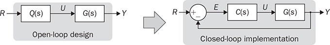
12.3 Affine Parameterization


12.3.1 Design Procedure
 , should be first defined according to the system requirement and the dynamic analysis of G0(s). Since the closed-loop transfer function is defined by (12.3), the intermediate function Q(s) is then derived by (12.6) for stability analysis. The transfer function of Q(s) should be stable and proper to indicate the internal stability of FQ(s) = Q(s)G0(s).
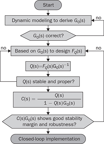

12.3.2 Desired Closed Loop


 and α1 =
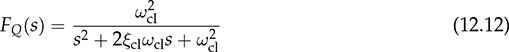
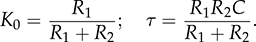
  . The parameters in FQ(s) should be specified, which include the damping ratio, ξcl, and the undamped natural frequency, ωcl. According to (12.12), the DC gain is assigned to one for the output to follow the reference command in steady states. The damping ratio is typically assigned to be from 0.7 to 2 to balance the response speed and overshoot level. The damping factor, ξcl, in FQ(s) is considered as the measurement of the oscillation scale in terms of the percentage of overshoot (PO) at the step response. The specification of ξcl can refer to Table 10.1, indicating the scale of overshoot. The ωcl is commonly chosen to be equal or higher than ωn for faster response. The settling time of the step response in the closed-loop system can be roughly approximated as
  , which is used to expect the closed-loop performance.


12.3.3 Derivation of Q(s) and C(s)
 and integral gain of


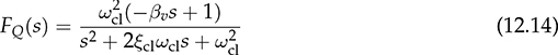
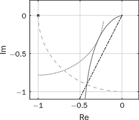
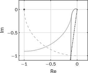
12.3.4 Relative Stability and Robustness

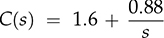
 . A feedback controller is designed to be the PI format and expressed as
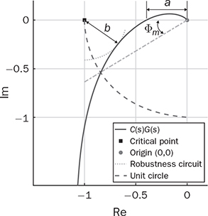
  . Using the “margin” function for C(s)G0(s), the phase margin is measured as Φm = 32.5° at the frequency of 0.76 rad/s. The phase margin is one indicator of the distance from the endless system oscillation. The gain margin is detected to be 2.52 in the absolute value or 8.02 in decibels (dB) at the crossover frequency of 1.29 rad/s. These stability margins can be shown by the Bode diagram of G0(s)C(s), as in Fig. 12.9, where both Φm and Gm are indicated.
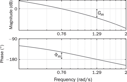
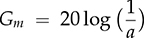 . The gain margin presents a different way to evaluate the relative stability and measure the distance from the endless system oscillation. The higher value of Gm or the lower value of a indicates a better stability.
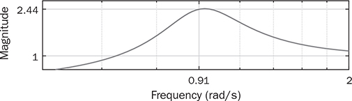

 leads to Φm = 32.5°, Gm = 8.02 dB, and max |So| = 2.44. When the controller gain is reduced by half and becomes
 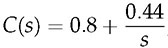 , the Nyquist plot of G0(s)C(s) is shown in Fig. 12.12 and indicates the increased margins as Φm = 57.91° and Gm = 14.04 dB. The sensitivity peak can be measured to be 1.57, lower than the previous case. This generally shows that the DC gain reduction of C(s) can improve the system stability and robustness. However, the control performance is accordingly reduced since a high DC gain of G(s)C(s) is desirable for the performance of fast dynamics response, effective disturbance rejection, and low steady-state error.
12.4 Controller Implementation
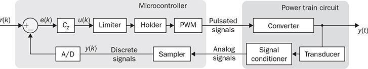
12.4.1 Digital Control
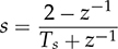 to replace “s” in the s-domain into “z.” The z-domain transfer function is related to the discrete-time operation regarding the specification of the sampling time, Ts. For example, the controller transfer function in (12.21) can be converted by the “c2d” function into the discrete format in (12.25).


12.4.2 PID Controllers
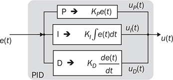


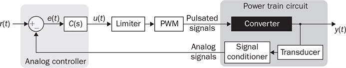
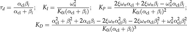
12.4.3 Analog Control


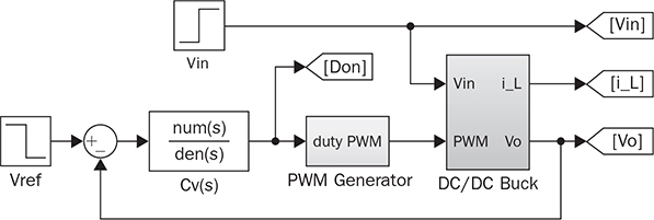
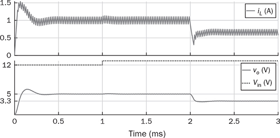
12.4.4 Case Study for Buck Converter


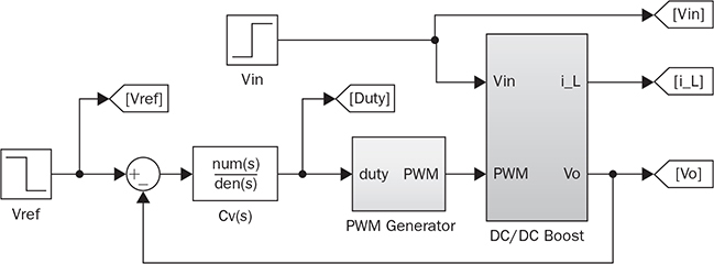
12.4.5 Case Study for Boost Converter


12.5 Cascade Control
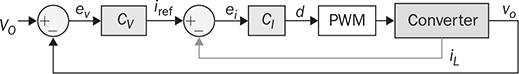
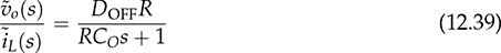
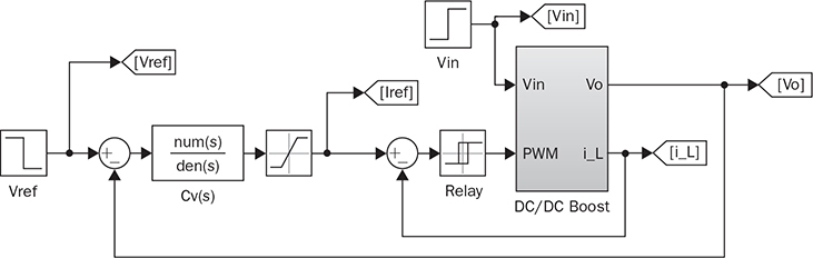
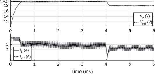
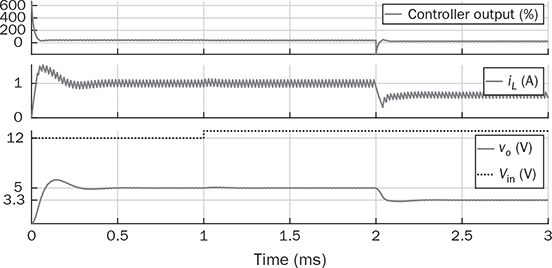
12.5.1 Case Study and Simulation

 and leads to a PI controller according to affine parameterization. The controller transfer function is derived as

12.5.2 Advantage
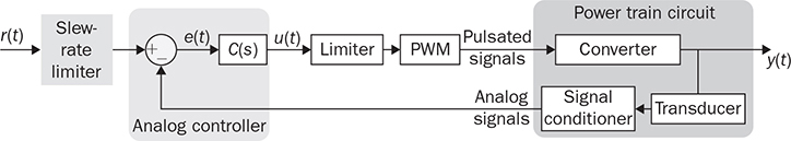
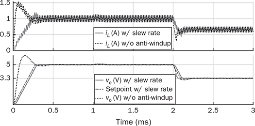
12.6 Windup Effect and Prevention
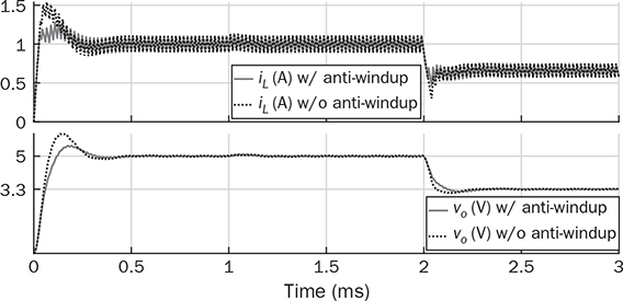
12.6.1 Case Study and Simulation
12.6.2 Anti-Windup
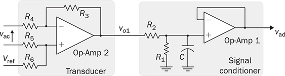
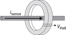
12.7 Sensing and Measurement

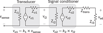
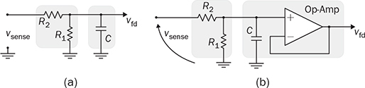
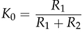
12.7.1 Voltage Sensing and Conditioning

 and
and 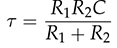 .
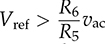
.
 . In the signal conditioning circuit, the voltage divider and filtering capacitor can be included for voltage scaling and noise mitigation. The transfer function of the signal conditioner is expressed in (12.43). The voltage follower is added in the end to ensure robustness for signal transmission. The zero-crossing detection of the AC voltage (vac) theoretically refers to the DC level of K0Vref represented by the signal, vad.


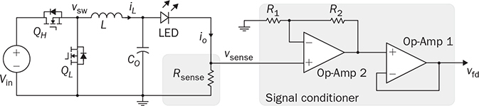
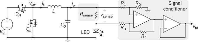
12.7.2 Current Sensing and Conditioning


12.8 Summary
Bibliography
Problems
 and
and  based on the