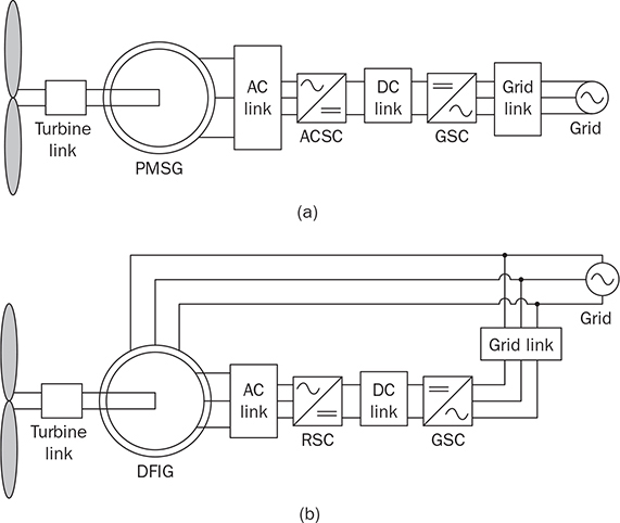
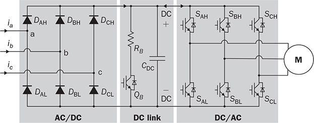
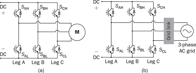
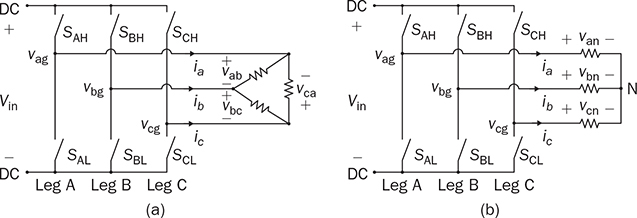
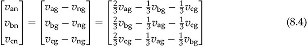
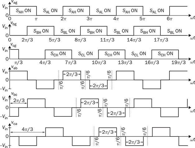
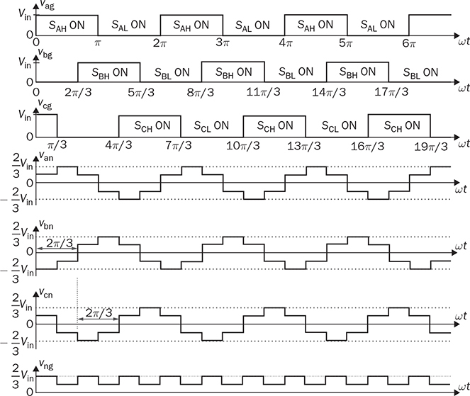
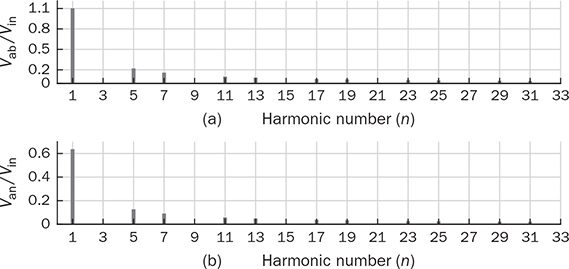
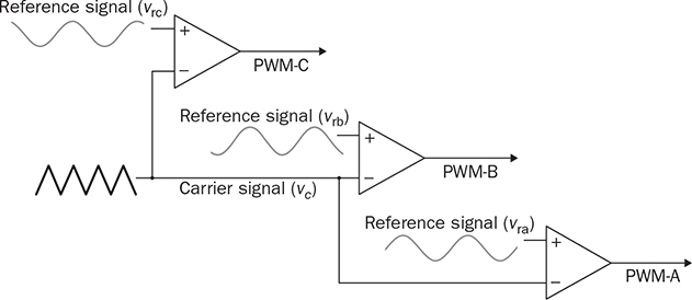
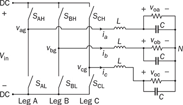
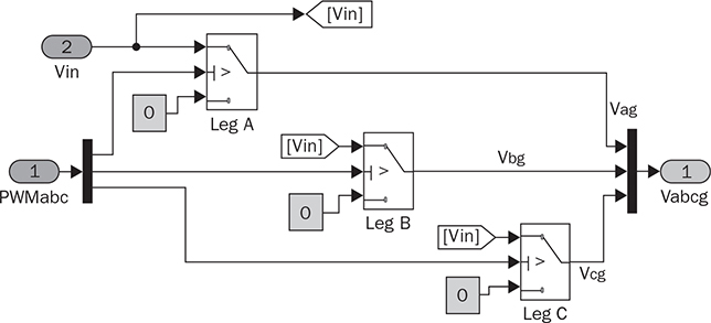
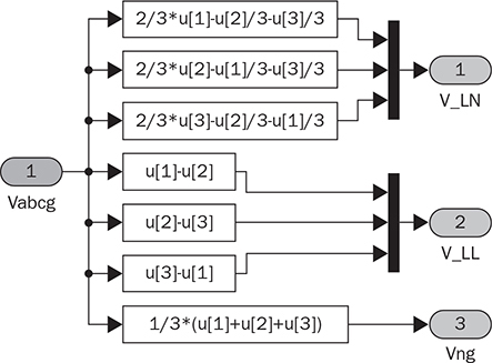
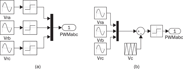
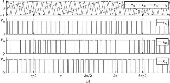
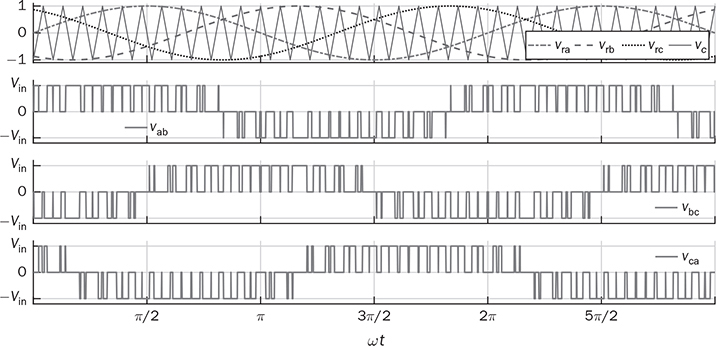
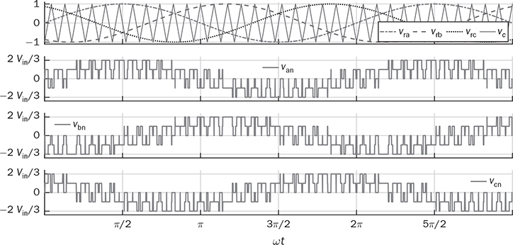
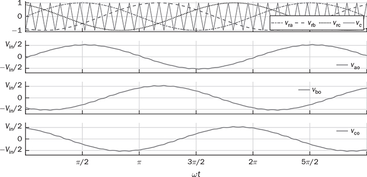
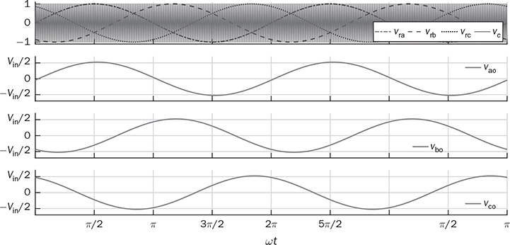
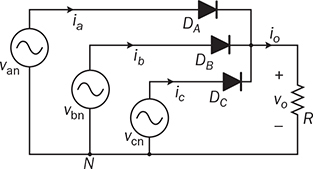
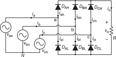
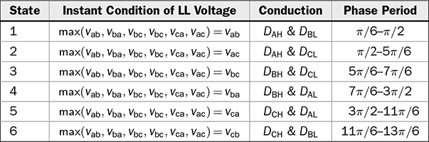
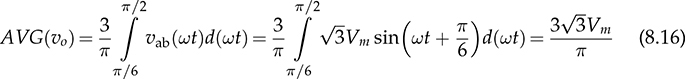
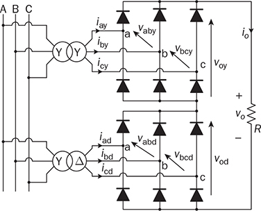
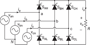
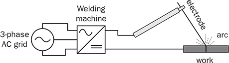
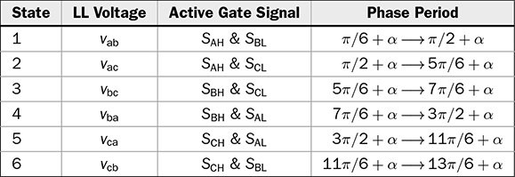
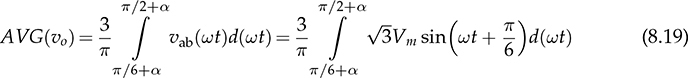
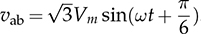
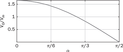
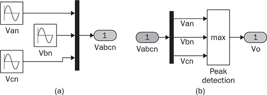
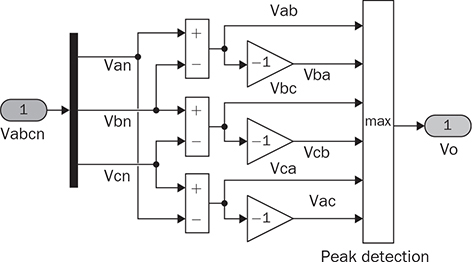
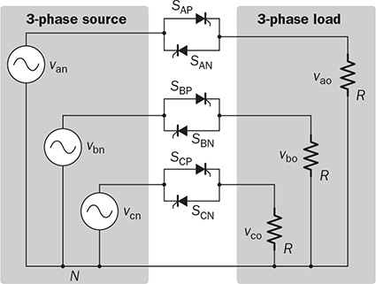
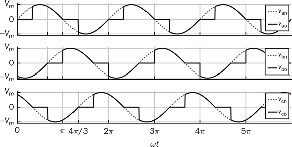
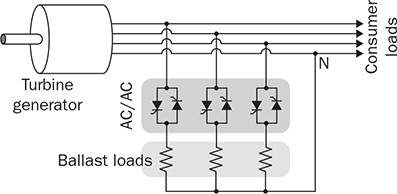
Three-phase AC provides great power density, which is commonly used for high-capacity systems and shows tremendous advantages. The power conversion between DC and three-phase AC is required for HVDC transmission systems. The wind power generation also follows such conversion stages between DC and three-phase AC, as illustrated in Fig. 8.1. The acronyms PMSG and DFIG represent the two common types of generators: the permanent magnet synchronous generator and doubly fed induction generator. Even if both directly produce three-phase AC, the AC/DC stages are required and shown as the AC side converter (ACSC) and rotor side converter (RSC). The DC link creates the path for active power to be converted and injected into the three-phase AC grid via the grid side converter (GSC). The conversion configuration adds more control functions to achieve the highest power generation, maintain the grid stability, and guarantee the power quality, regardless of the variation of the wind speed or other disturbance. FIGURE 8.1 Illustration of wind power systems using (a) PMSG; (b) DFIG. Electric motors that show high efficiency and high capacity mostly refer to the three-phase AC types. Even though the three-phase AC supply can directly power such motors, the system requires a variable frequency drive as a power interface to achieve the best performance. Figure 8.2 shows the typical back-to-back configuration of circuits for motor-driving applications. The power flow goes through the AC/DC conversion, DC link, and DC/AC conversion. The two-stage conversion of AC/DC and DC/AC is complicated since it requires a significant number of power switches. However, it provides the mechanism to achieve the best utilization of different three-phase AC motors regarding the fully controllable speed and torque. Therefore, the power conversion between DC and three-phase AC is an important subject for power electronics and system applications. FIGURE 8.2 Variable frequency drive for motors with braking resistor and chopper. The increasing utilization of batteries and renewable energy resources requires more and more DC to three-phase AC conversion to supply grids. The boom of electric vehicles (EVs) also demands high performance from the DC/AC conversion to drive electric motors. The typical bridge circuit for DC to three-phase AC conversion has been introduced in Sec. 2.4 and shown in Fig. 2.15c. The six-switch bridge shows three legs, A, B, and C, each formed by the high- and low-side active switches, as shown in Fig. 8.3. Even though the same bridge circuit is applied, the term can be different depending upon the type of applications. For example, the term “voltage source inverter (VSI)” is commonly used for motor drive applications, as illustrated in Fig. 8.3a. The term “current source inverter (CSI)” is used for interfacing power generation into the three-phase AC grid, as shown in Fig. 8.3b. The difference in modulation and operation causes the same bridge circuit to have different names, such as VSI and CSI. In this book, the active six-switch bridge is mostly discussed to avoid the confusion. IGBTs commonly are used to construct the bridge circuits for high-power ratings. FIGURE 8.3 Six-switch bridge for DC to three-phase AC conversion to support (a) AC loads; (b) grid interconnection. Following the circuit in Fig. 8.4, the six states of the switching operation and the voltage response can be defined by FIGURE 8.4 Six-switch bridge for DC to three-phase AC conversion for different load connections: (a) delta; (b) wye. • On-state of SAH ⇒ off-state of SAL ⇒ vag = Vin • On-state of SAL ⇒ off-state of SAH ⇒ vag = 0 • On-state of SBH ⇒ off-state of SBL ⇒ vbg = Vin • On-state of SBL ⇒ off-state of SBH ⇒ vag = 0 • On-state of SCH ⇒ off-state of SCL ⇒ vcg = Vin • On-state of SCL ⇒ off-state of SCH ⇒ vcg = 0 For the three-phase AC output, the load can be connected as either delta or wye, as shown in the equivalent circuits illustrated in Fig. 8.4. For the delta connection, the direct line-to-line (LL) voltage is applied to the three-phase load resistors and expressed by For the wye connection of the load, a neutral point is presented and shown in Fig. 8.4b. According to Kirchhoff’s current law (KCL), we have ia + ib + ic = 0. The voltage potential between the neutral point and the DC ground is symbolized as vng. Regarding a balanced three-phase load, the value of vng can be derived from (8.2) into (8.3). where R is the load resistance, equal for the three phases. Therefore, the line-to-neutral (LN) voltage of the three phases can be determined by (8.4). A simple modulation scheme can be created so that each active switch is switched based on the fundamental frequency of the AC output. When the 50% duty cycle for the on/off switch is applied, it refers to the 180° on-state in the phase domain. The phase delay of FIGURE 8.5 Waveforms of 180° modulation for LL voltage output. Figure 8.4b shows the case in which the three-phase load is connected across the LN voltages. Figure 8.6 illustrates the waveforms of the LN voltages, van, vbn, and vcn, where the 180° modulation is applied. The voltage between the neutral point to the DC ground is plotted, which is symbolized as vng. The voltage level in each step of van, vbn, and vcn can be determined according to (8.4). The LN voltage waveforms show four levels: FIGURE 8.6 Waveforms of 180° modulation for LN voltage output. The simple 180° modulation can operate the six-switch bridge to produce three-phase AC output. The switching frequency is the same as that of the output AC. Compared to other modulation technologies, the advantage lies in the simple switching operation and low switching frequency. The main concern is the distortion from the sine wave to represent the ideal AC signal in power systems. According to the Fourier series, the amplitude of the fundamental frequency component is computed by (8.8). Following the waveforms in Fig. 8.5, the THD level of the LL voltage is found to be 31% by using (4.24). The frequency spectrum illustrates the individual harmonic components, as shown in Fig. 8.7a. FIGURE 8.7 Harmonic spectrum of the AC voltage produced by 180° modulation: (a) LL; (b) LN. Regarding the LN voltage, as shown in Fig. 8.6, the amplitude of the fundamental frequency component can be computed by (8.9). The harmonic distribution is illustrated in Fig. 8.7b. The THD value of the LN voltage can be measured to be 22%. According to the THD analysis, the amplitude of the third-order harmonic component is zero. The dominant frequency of the harmonics is represented by the fifth-order, as shown in Fig. 8.7. Meanwhile, the harmonics with the multiple of the third order are also absent from the spectrum. The 180° modulation represents the highest voltage output based on the six-switch bridge for a DC to three-phase AC conversion. It is a simple solution, but shows high THD. The sine-triangle modulation can be applied to produce three-phase AC for higher power quality. Similar to the sinusoidal pulse width modulation (SPWM) for DC to single-phase AC, the modulation can be constructed and shown in Fig. 8.8. The technology is commonly called the three-phase SPWM. The reference signals, vra, vrb, and vrc, show the three-phase sinusoidal waveforms indicating the phase difference of FIGURE 8.8 Principle of sine-triangle modulation for DC to three-phase AC. The three PWM signals are applied to the six-switch bridge circuit corresponding to the three legs A, B, and C, as shown in Fig. 8.4. Table 8.1 summarizes the switching operation and the resulting output based on the sine-triangle modulation. Figure 8.9 shows one configuration with the LC filtering to supply the wye-connected load. The modulation index, ma, is the controlled variable to determine the output voltage level. The LN voltages, voa, vob, and voc, are expected to be sinusoidal waveforms. When loss is neglected, the amplitude of LN voltages crossing the load shall be proportional to the modulation index of amplitude, ma. Thus, the expression of the LN voltage is shown in (8.10)–(8.12), where 0 ≤ ma ≤ 1. The amplitude of FIGURE 8.9 DC to three-phase AC conversion with LC filtering for wye loads. TABLE 8.1 Sine-Triangle Modulation for DC to Three-Phase AC The active six-switch bridge includes three legs, namely, A, B, and C. The Simulink model can be built to reflect the three-leg configuration, as shown in Fig. 8.10. Each leg is represented by the single-pole-double-throw (SPDT) switch to simulate the switching logic between the upper and lower switches. The legs are controlled by the switching command signals, PWM-A, PWM-B, and PWM-C, which are multiplexed and shown as one input “PWMabc.” The model output includes the three-phase voltage signals vag, vbg, and vcg, which are multiplexed into one signal “Vabcg.” The voltage level is either Vin or 0, depending on the modulation signals. FIGURE 8.10 Simulink model for active six-switch bridge. The voltage potential of vag, vbg, and vcg can result in either LL or LN voltage, depending on load configurations. Figure 8.11 shows a general computation model that is built by the mathematical expressions for voltage outputs in (8.1), (8.3), and (8.4). The three-phase LL and LN voltages are multiplexed into “V_LN” and “V_LL” to simplify the model presentation. The neutral-to-ground voltage is also computed as the output, which is shown as “Vng.” FIGURE 8.11 Simulink model to compute the LL and LN voltage output. Figure 8.12a shows the simulation model formed for the 180° modulation. The operation of sine-triangle modulation is modeled by Simulink and illustrated in Fig. 8.12b, where the carrier signal is the triangle waveform and shown as vc. The reference signal for SPWM is shown as vra, vrb, and vrc with the phase difference of FIGURE 8.12 Simulation model for DC to three-phase AC modulation: (a) 180°; (b) sine-triangle. For the 180° modulation, the simulation result has been shown in Figs. 8.5 and 8.6 to represent the LL and LN voltage output, respectively. The output voltage level is fixed with the input voltage, Vin. The frequency follows the reference signals vra, vrb, and vrc with the phase difference of Another case study simulates the sine-triangle modulation for DC to three-phase AC conversions. The parameter setting is just for demonstration purpose, which shows the modulation indices ma = 1 and mf = 23. Figure 8.13 shows the pulsating waveforms of vag, vbg, and vcg, resulted from the SPWM. Each phase shows 23 voltage pulses in every AC cycle. The switching frequency is 23 × ω, where ω refers to the fundamental frequency of the AC output in rad/s. Figure 8.14 illustrates the simulated result regarding the LL voltage output when SPWM is applied. When the load is connected in wye, the LN voltages would be as shown in Fig. 8.15 and modulated by the SPWM. FIGURE 8.13 Switching demonstration of DC to three-phase AC conversion by SPWM. FIGURE 8.14 Simulated LL voltage produced by SPWM. FIGURE 8.15 Simulation result of LN voltage produced by SPWM. When the LC filter is applied to the load side, as shown in Fig. 8.9, the low-pass filter design can follow the early analysis in Sec. 2.7. The circuit can be simulated based on the same modulation index as in the case study. Following Fig. 8.9, the circuit parameters are as follows: L = 5 mH, C = 100 μF, and R = 20 Ω. The simulated voltages crossing the loads are illustrated in Fig. 8.16, which clearly shows the shape of sine waveforms. The output amplitude can be adjusted by changing the value of ma. In practical systems, the setting of mf is much higher than 23 to achieve a wide separation between the fundamental frequency and the switching frequency. It is an effective way to improve the power quality and reduce the size of low-pass filters. Figure 8.17 illustrates the simulation result of the voltage crossing the wye-connected load when mf = 223. Compared to Fig. 8.16, the improvement is clear even though the filtering circuit is scaled down to L = 500 μH and C = 10 μF. Further, the amplitude of LN voltages is FIGURE 8.16 LN voltage crossing the load after low-pass filtering with the parameters of mf = 23, L = 5 mH, C = 100 μF, and R = 20 Ω. FIGURE 8.17 LN voltage crossing the load after low-pass filtering with the parameters of mf = 233, L = 500 μH, C = 10 μF, and R = 20 Ω. The conversion from three-phase AC to DC is typical for HVDC transmission systems and high-power applications, such as motor drives. Future DC grids demand more of the three-phase AC to DC conversions to interconnect with efficient AC generators. Figure 8.18 shows a diode implementation, where the source and load share the common neutral point. The circuit supports the peak-detection operation that the highest LN voltage causes its corresponding diode to be forward-biased. The other two are reverse-biased due to the lower voltage potential. The DC output vo rides on the peak of the positive voltage cycle among the three LN voltage signals, which is illustrated in Fig. 8.19. Three pulses are equally divided and appear in each 2π cycle of the AC waveform. Thus, the topology commonly refers to as the three-pulse rectifier. FIGURE 8.18 Three-phase rectifier for three pulses per cycle. FIGURE 8.19 Waveforms of passive rectifier showing three pulses per cycle. The averaged value of the DC output can be computed by (8.13), which is about 0.83Vm in value. The RMS value of vo can be derived by (8.14), which is about 0.84Vm. The value of Vm stands for the amplitude of the LN voltage, which is the highest of vo. The transition moment from one phase to another indicates the lowest values of vo. The commutation points are indicated by Fig. 8.19 as A six-diode bridge is common to construct the three-phase AC to DC conversion. Figure 8.20 illustrates the six-switch bridge configuration and includes both the source and load. The configuration performs peak detection, which selects highest voltage among the six LL voltage: vab, vba, vbc, vbc, vca, and vac. The highest LL voltage makes one diagonal pair of diodes forward-biased to deliver DC voltage to the load. The rest of the diodes are reverse-biased due to the lower voltage potential. FIGURE 8.20 Three-phase bridge rectifier for six pulses per cycle. Table 8.2 defines the six conduction states, which are cycling among the six LL voltages. The rectification waveforms are illustrated in Fig. 8.21. The LN voltages are plotted for the reference since vab = van − vbn; vac = van − vcn; vba = vbn − van; vbc = vbn − vcn; vca = vcn − van; vcb = vcn − vbn. At any given time, two diodes are conducting simultaneously, one from the high-side group and another from the low-side group. The highest voltage among the six LL voltages appears at the load side. The topology is often called a six-pulse rectifier since six pulses are clearly shown in one 2π cycle of the output voltage, vo. TABLE 8.2 Operation of Three-Phase AC to DC Conversion with Six Pulses The average value of the output can be derived according to the waveform of vo and expressed by (8.16). The value is about 1.65Vm, where van = Vm sin(ωt). FIGURE 8.21 Waveforms of the three-phase bridge operation showing six pulses per cycle at the output. The peak-to-peak ripple of vo is determined by (8.17), according to the waveforms shown in Fig. 8.20. It counts as 14% of the averaging value of vo. The twelve-pulse rectifier utilizes the stack technology and transformer winding configuration to create an advanced conversion. Figure 8.22 illustrates the rectifier configuration, which is widely used for three-phase AC to DC conversion in power systems. The Y-Y-configured transformer does not introduce a phase difference between input and output. However, the Y − Δ transformer introduces a 30° or FIGURE 8.22 Three-phase bridge rectifier using diodes for 12 pulses of output. FIGURE 8.23 Waveforms of the three-phase bridge showing the phase difference. Each six-switch bridge performs the peak detection operation to pick the highest among the six LL voltages. The six pulses in one bridge output are clearly shown in Fig. 8.23. The DC voltages are symbolized as voy and vod to represent outputs of the upper and lower bridge, respectively. The stack configuration of the two bridges makes the final output, vo = voy + vod, as shown in Fig. 8.24. Due to the phase shift of π/6, the terminal output, vo, shows 12 pulses per line cycle, which gains the name of the 12-pulse rectification. The DC voltage level is the sum of the outputs of the two 6-pulse bridge rectifiers. Figure 8.24 shows the output voltages are equally distributed by the two bridges. The peak-to-peak ripple of vo can be determined by (8.18). The ripple of the 12 pulses weigh about 1.8% of the averaging voltage of the output without filtering. Thus, the 12-pulse rectification is an effective way to increase the DC voltage level and reduce the ripple weight. Filtering can be implemented to improve DC power quality further. FIGURE 8.24 Waveforms of three-phase bridge configuration to produce 12 pulses per cycle. Diode-based rectifiers are incapable to control the output voltage. The chopping operation using silicon controlled rectifiers (SCRs) can be applied to the three-phase AC to DC conversion, which regulates the DC output vo to a lower level. A six-switch bridge formed by SCRs is shown in Fig. 8.25. The delayed phase angle (α) can be applied to control the conduction of each SCR and chop the output voltage waveform. FIGURE 8.25 Three-phase bridge rectifier using SCR for output voltage regulation. The active six-switch bridge is widely used as the DC power supply for arc welding, which is a fusion process for melting and joining metals. Figure 8.26 illustrates the operation, where significant DC current is required to produce arc and intense heat. The DC output is regulated by the firing angle on SCRs to the required level and meets the welding requirement. FIGURE 8.26 Demonstration of arc welding operation. Without any phase delay, the DC output is the highest and equivalent to that of the diode-based bridge. When the phase control is applied, the delayed phase angle can be recognized by the firing signals to the six SCRs in the bridge for switching. Table 8.3 provides the conduction time period of the controlled LL voltage corresponding to the diagonal pair of the active switches. The averaging value of the output voltage is determined by (8.19) based on the waveform of vab and the conduction time of TABLE 8.3 Operation of Three-Phase AC to DC Conversion with Controlled Six Pulses SAH and SBL. The voltage level is expressed by (8.20) that is controlled by the assigned α. The phase control performs step-down conversion from the highest value, where the LN voltage of phase A is expressed by van = Vm sin(ωt) and the LL voltage is FIGURE 8.27 Voltage regulation ratio by delayed phase angle, α. The above introduction and analysis of the phase control are based on a six-pulse rectifier. The same operation using SCRs can be applied to other rectifier topologies, such as the 3-pulse rectifier and 12-pulse rectifier. First, the diode-based bridges are replaced by the active bridges using SCR. Second, the delayed fire angle can step down the output voltage to the desired level. Filtering can be implemented to improve power quality in the AC and DC sides. Figure 8.28 illustrates the Simulink models for the three-pulse rectification using diodes. The three-phase LN voltages are multiplexed into an integrated signal, as shown in Fig. 8.28a. The peak detection mechanism of the LN phase voltages is represented in Fig. 8.28b. Figure 8.29 illustrates the Simulink model for the six-pulse rectifier using diodes. The inputs are the three-phase LN voltages, which lead to the six LL voltages. The “max” block in Simulink performs peak detection to output the rectified voltage, VO. FIGURE 8.28 Simulink models for three-phase AC to DC conversion: (a) LN voltage source; (b) three-pulse rectifier. FIGURE 8.29 Simulink models of six-pulse rectifier for three-phase AC to DC conversion. Phase-controlled three-phase AC can support voltage regulation, which has been traditionally used for various applications, such as stove burner, and speed control of three-phase motors. On topology is the series voltage regulator, the concept of which is demonstrated in Fig. 8.30. The delayed fire angle for SCRs can be controlled to chop the three-phase AC waveform and reduce power output and the voltage across the load. For each phase, a pair of SCRs are connected antiparallel in order to achieve controlled rectification in both directions. Figure 8.31 demonstrates the chopped three-phase AC waveforms resulted from the phase control operation. FIGURE 8.30 Demonstration of three-phase voltage regulation in wye connection. FIGURE 8.31 Waveforms of three-phase voltage regulation in wye connection. One practical application is the shunt voltage regulator to control a stand-alone micro-hydro power generation. Figure 8.32 shows the system diagram, including the key components of the turbine generator, shunt regulator, and ballast loads. Low-cost micro-hydro power plants do not control water flow due to mechanical difficulty and slow dynamic response. Thus, the voltage regulation is based on the three-phase AC/AC conversion and the three-phase AC voltage controller, as shown in Fig. 8.32. The operation dumps excessive power to the ballast load in order to maintain the three-phase bus for the required level. The three-phase AC voltage controller operates SCRs and the ballast loads to balance the power generation and power consumption. The system can respond fast to maintain steady three-phase AC voltage against disturbance from the consumer loads. The extra power generation is simply wasted, which shows the application’s drawback. FIGURE 8.32 Phase-controlled three-phase AC circuit for voltage regulation. The phase control is an old technology, which shows poor power quality. Advanced solutions for the AC/AC conversion are available because of the development of power electronics. One topology follows the two-stage conversion or back-to-back configuration, as illustrated in Fig. 8.2. The intermediate DC link between two bridges creates the energy buffer for active power transmission. The active bridge serves as the driver to be implemented by advanced modulation and control. The DC link includes a protection circuit to avoid overvoltage in case the motor rotation energy returns. A typical solution is shown as the braking resistor circuit to dissipate any extra energy. The wind-generated power is also transmitted to grids through the AC/DC/AC stage discussed earlier in the chapter and illustrated in Fig. 8.1. Even though the structure is more complicated than the phase control configuration using SCRs, the back-to-back solution shows the advantages of advanced control, high efficiency, optimal operation, and high performance. Three-phase AC represents the backbone of power systems and electric machine applications. The recent trend shows that the conversion between DC and three-phase AC is demanded by the implementation of wind power generation and utility-scale energy storage. The subject has been well presented in textbooks of power systems and electric machines. This chapter has introduced fundamental information on power conversion systems regarding the three-phase AC. The discussion includes the AC/DC, DC/AC, and AC/AC conversions. The DC to three-phase AC conversion shows an increasing trend to interface grids with more and more distributed renewable power generation and energy storage. Such conversion is typically based on the active six-switch bridge and modulated for different functions. The chapter covers the techniques of the 180° modulation and SPWM. More advanced techniques are also available, such as the space vector modulation, which can maintain low switching frequency but control good power quality. The three-phase AC to DC conversion covers the 3-pulse, 6-pulse, and 12 pulse configurations. The topology selection is based on the specified voltage and power level. The rectification shows the DC output ripple is lower than that of the single-phase AC to DC cases. It generally shows the advantage of three-phase AC system interconnecting with DC power applications. The stress of the filtering circuit is low for such conversions. The phase control technique using SCRs is a traditional way to regulate power and voltage output. However, the low-cost solution raises the concern of power quality and limited control capability. The advances in power electronics lead to a comprehensive solution, including the AC/DC, DC link, and DC/AC conversion. Power quality can be satisfied to support the grid interconnection and load requirement. Modern power electronics indicates a high potential to reform the traditional power network. 1. C-M. Ong, Dynamic simulation of electric machinery using Matlab/Simulink, 1st ed., Prentice Hall, 1997. 2. W. Xiao, Photovoltaic power systems: modeling, design, and control, 1st ed., Wiley, 2017. 8.1 Follow the case study discussed in this chapter and build your own simulation models to study the DC to three-phase AC conversion. Simulate the operation of the bridge circuit with the 180° modulation, sine-triangle modulation, and low-pass filtering circuit. 8.2 Follow the case study discussed in this chapter and build your own simulation models to study the three-phase AC to DC conversion. Simulate the passive rectifiers to output three pulses per cycle and six pulses per cycle. 8.3 Search academic publications to find other topologies to achieve the DC to three-phase AC conversion.
CHAPTER 8

Conversion Between Three-Phase AC and DC
8.1 DC/AC Conversion
8.1.1 Bridge and Switching Operation


8.1.2 180°Modulation
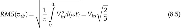
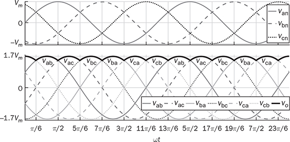
 or 120° should be applied among the three phases, namely, A, B, and C. Figure 8.5 demonstrates the three-phase waveforms regarding the voltages of vag, vbg, vcg, vab, vbc, and vca, which are produced by the 180° modulation. All variables are referred to in Fig. 8.4a. Following the waveform of vab in Fig. 8.5, the root-mean-square (RMS) value can be determined by (8.5), where
  . The same RMS computation is applied to another two LL voltages.
 Vin,
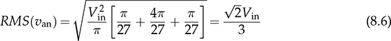
Vin, 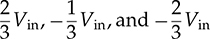 . Six steps of the LN voltage appear and are distributed equally in each 2π cycle. The RMS value can be computed by (8.6). It can also be derived by (8.7) when the RMS value of the LL voltages is available.


8.1.3 Sine-Triangle Modulation
 . Each is assigned to the amplitude, ma, and fundamental frequency, ω. Therefore, the math ematical expressions are: vra = ma sin(ωt), vrb = ma
  ), vrc = ma
  ). The carrier signal, vc, is a triangle wave with the peak-to-peak amplitude of ±1 and
 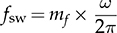 . The ma and mf represent the modulation indexes for the output amplitude and switching frequency.
 can be achieved in theory when ma = 1, which is based on the equivalence of the load neutral point with the center-tapped DC voltage, Vin.


8.1.4 Modeling for Simulation
 in between. The comparison between the reference signals and the carrier produces PWM signals to control the six switches.
8.1.5 Case Study and Simulation Result
 in between.
 , in response to the modulation index for amplitude, ma = 1.
8.2 AC/DC Conversion
8.2.1 Passive Rectifier for Three Pulses per Cycle
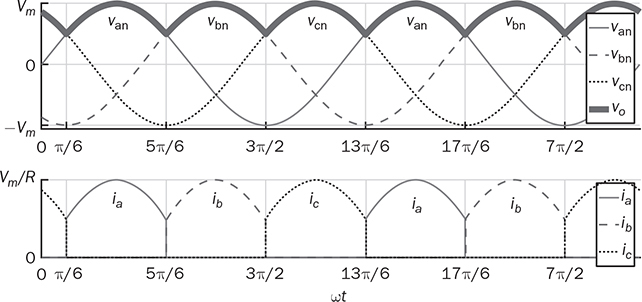
 in each line cycle. The peak-to-peak voltage ripple of vo is known as
  which is expressed in (8.15). Each phase equally shares the power contribution in the three-phase manner. The phase current is symbolized as ia, ib, and ic, as indicated in Fig. 8.18 and plotted in Fig. 8.19. The load current, io, is equally contributed by the three-phase current.


8.2.2 Passive Rectifier for Six Pulses per Cycle

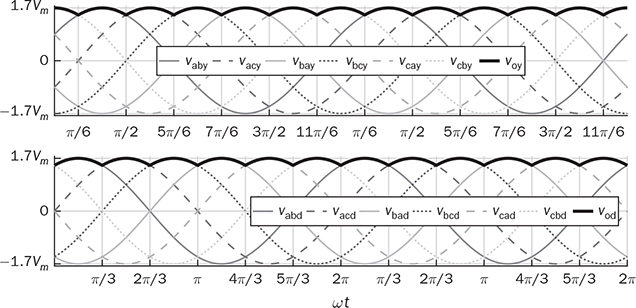
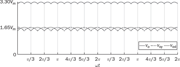
8.2.3 Passive Rectifier for 12 Pulses per Cycle
 6 phase shift. The phase difference can follow the phasor diagram, as demonstrated in Fig. 1.11b. The waveforms of the two-bridge operation are shown in Fig. 8.23.

8.2.4 Active Rectifier
 , when α = 0.
 . The conversion ratio is plotted in Fig. 8.27, where VO represents the averaged value of the DC output, vo. The peak-to-peak voltage ripple increases due to the chopping operation when α ≠ = 0.

8.2.5 Simulation
8.3 AC/AC Conversion
8.4 Summary
Bibliography
Problems