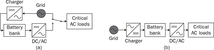
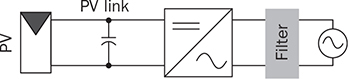
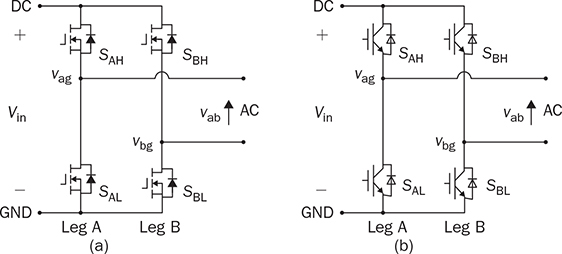
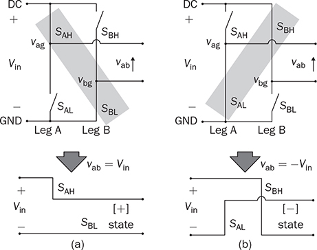
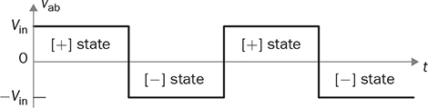
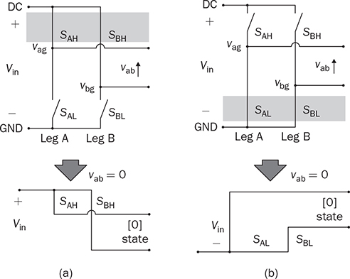
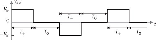
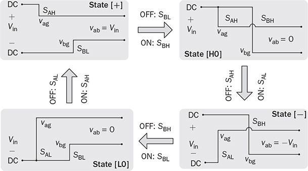
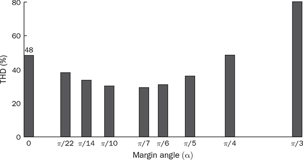
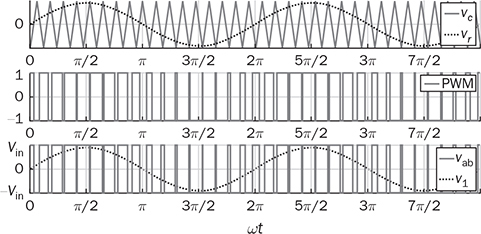
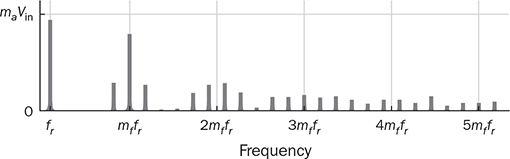
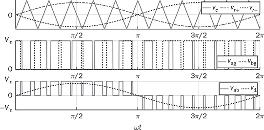
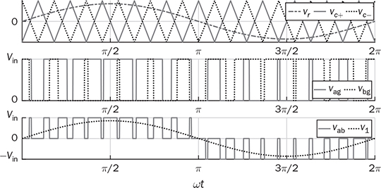
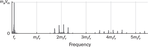
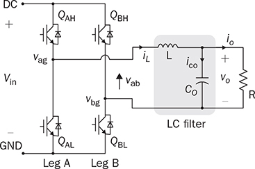
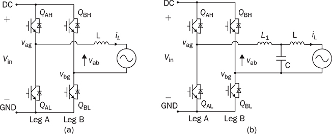
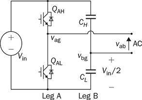
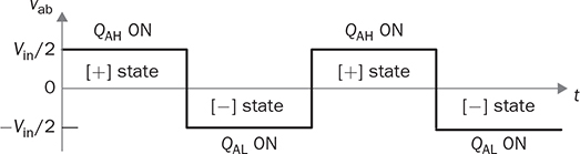
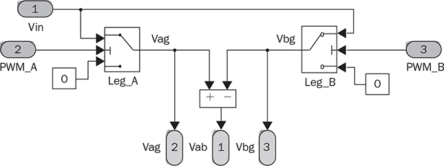
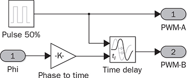
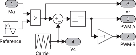
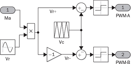
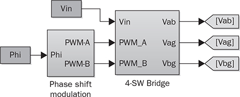
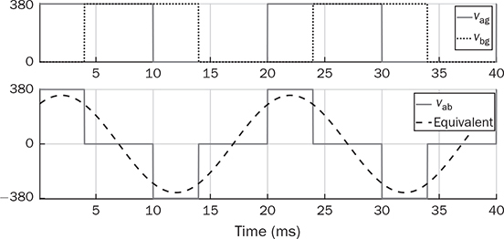
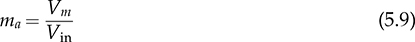
DC to single-phase AC conversion has been widely used for battery-powered power supplies. The device to perform DC/AC conversion is often called an inverter. The examples include the uninterrupted power supplies (UPS) for critical loads and inverters powered by car batteries. Such systems generally work on low power capacity to supply single-phase AC directly to loads. Figure 5.1 illustrates two types of UPS: offline and online. FIGURE 5.1 Block diagram of uninterrupted power supplies: (a) standby; (b) online. In the offline system or so-called standby UPS, the single-pole-double-throw (SPDT) relay connects the critical load with the grid supply, as shown in Fig. 5.1a. The battery bank remains charged through a charger, which performs AC/DC conversion when the grid supply is available. When a power outage happens, the DC to single-phase AC is activated to convert DC power from the battery and supply critical AC loads. The DC/AC inverter is mostly standby without any power conversion. The drawback of standby UPS lies in the transition time of the SPDT and the start-up of the inverter. A short-time delay is always present during the transition from the grid to the inverter output. The delay is short enough to keep desktop computers working without any interruption. Solid-state relays are constructed by power semiconductors that can shorten the transition time to replace the mechanical relay. The online UPS system can eliminate the transition time and make the DC/AC converter work full-time to support the load, as shown in Fig. 5.1b. The battery bank becomes a DC interlink between the charger and the DC/AC conversion. During a sudden power outage, the charger stops to operate but the DC/AC conversion is not interrupted and shows a seamless transition. However, the stress on both the AC/DC and DC/AC converters is high due to the full-time power process. The solution generally costs higher than the standby counterpart. The DC/AC conversion for UPS belongs to the stand-alone systems that provide power to single-phase AC loads and maintain the output voltage and frequency. Nowadays, another category of DC to single-phase AC conversion is used for the AC grid interconnection with renewable energy resources. The most common application is the photovoltaic (PV) grid-tied system, which has grown dramatically for home and building installations around the world. Figure 5.2 shows a simplified system diagram, where the PV generator produces DC power. The solar power is converted to single-phase AC and then injected into the public power distribution network. FIGURE 5.2 Simple version of grid-tied PV power system. The most common topology is the active four-switch bridge for DC to single-phase AC conversion, which has been introduced in Sec. 2.4 and illustrated in Fig. 2.15b. The bridge topology is typically constructed by either field effect transistors (FETs) or insulated gate bipolar transistors (IGBTs), as shown in Fig. 5.3. The switch selection depends on the power and voltage level, as discussed in Sec. 2.3.5. The four-switch bridge is formed by two legs in parallel, marked as A and B. The AC output is expressed by vab = vag − vbg, where vag and vbg show the voltage potential to the common DC ground of Leg A and Leg B, respectively. The voltage potential difference leads to the AC output, vab. When one switch is turned on, another in the same leg should be synchronously switched off to avoid any cross conduction or shoot through. FIGURE 5.3 Bridges for DC to single-phase AC conversion by (a) FETs; (b) IGBTs. The on/off switching is feasible to produce square waveforms. The diagonal switching patterns of the four-switch bridge can produce either the positive or negative output at the AC terminal, as illustrated in Fig. 5.4. For the positive cycle, the output is vab = Vin − 0 = Vin formed by the conduction of the diagonal pair of SAH and SBL. The onstate of SBH and SAL leads to the negative cycle, where vab = 0 − Vin = −Vin. The output voltage, vab, becomes an AC waveform when the two cycles are equally split, as shown in Fig. 5.5. The simple switching mechanism starts the DC to single-phase AC conversion. FIGURE 5.4 Diagonal conduction of four-switch bridges for DC/AC conversion: (a) [+] state; (b) [−] state. FIGURE 5.5 Square AC waveform produced by active four-switch bridge. The switching operation is simple to produce square AC waveforms through the four-switch bridge and follow a specified frequency, e.g., 50 or 60 Hz. Nevertheless, the modulation is incapable of regulating the output AC voltage, vab. The amplitude and RMS values of vab are fixed to the DC level of Vin. Based on the four-switch bridge in Fig. 5.3, another two switching states can be achieved to produce cycles with zero output voltage. Figure 5.6 illustrates the two states, which are also called the flat switching pattern. Either the high-side or low-side switches are on-state at the same time, which leads to vab = vag − vbg = 0. The zero states are defined as [H0] and [L0] to distinguish the on-states of both high-side switches and low-side switches, respectively. When the two zero states are introduced in between the state [+] and state [−], the chopped square waveform can be produced for vab, as shown in Fig. 5.7. The marks of T+, T−, and T0 represent the periods of the positive, negative, and zero state, respectively. The RMS value of vab becomes controllable by adjusting the state periods. FIGURE 5.6 Flat conduction states of the four-switch bridge for DC/AC conversion: (a) [H0] state; (b) [L0] state. FIGURE 5.7 Chopped square AC waveform produced by four-switch bridge. Modulation can generate the switching sequence described as the following: 1. SAH switched on ⇒ SAL off ⇒ vag = Vin & vbg = 0 ⇒ vab = Vin ⇒ state [+]. 2. SBH switched on ⇒ SBL off ⇒ vag = Vin & vbg = Vin ⇒ vab = 0 ⇒ state [H0]. 3. SAH switched off ⇒ SAL on ⇒ vag = 0 & vbg = Vin ⇒ vab = −Vin ⇒ state [−]. 4. SBH switched off ⇒ SBL on ⇒ vag = 0 & vbg = 0 ⇒ vab = 0 ⇒ state [L0]. At each switching moment, one switch is turned on, and another on the same leg is automatically turned off. Each switch maintains on-state for half cycle or 50% duty cycle, which results in rectangular waveforms of vag and vbg. A time delay is applied between the switching-on of SAH and SBH. The time delay represents the period of the positive state, which is equal to that of the negative state. Figure 5.8 demonstrates the equivalent circuits in response to the switching sequence. FIGURE 5.8 Switching sequence to produce chopped square waveform. The above operation can be explained in the phase domain, as shown in Fig. 5.9. Phase shift between two rectangular waves is a common modulation technique that can produce the chopped square waveform for the DC to single-phase AC conversion. The phase value is represented by Φ for analysis, which is indicated in Fig. 5.9. The pulse width of the states [+] and [−] corresponds with Φ in each 2π cycle. The zero states, [H0] and [L0], lead to zero output voltage. The RMS value of the output AC voltage is regulated by the phase-shift angle. Based on one half-cycle in steady state and the waveform shown in Fig. 5.9, the RMS value of vab can be derived by When Φ = 0, the rectangular waveforms of vag and vbg are overlapped and result in zero output of vab. When Φ = π, the square waveform appears and represents the highest voltage conversion ratio from DC to single-phase AC. When FIGURE 5.9 Phase shift to produce single-phase AC waveform. FIGURE 5.10 Equivalence of sine wave with chopped square waveform. To match and compare with the sine wave, the pulse of the chopped square waveform is centered in each half-cycle, as shown in Fig. 5.10, when The phase shift technology can modulate the four-switch bridge to produce single-phase AC output with controllable voltage output. The main concern results from the distortion in comparison with the ideal AC signal in power systems. The total harmonic distortion (THD) has been introduced in Sec. 4.5.2 to quantify the difference. For the chopped square waveform, vab, the Fourier transform (FT) series is expressed by where the fundamental frequency refers to ω0, and the odd number of harmonics is counted. The amplitudes for the n odd harmonic component of the chopped square waveform is expressed by (5.4). The amplitude and RMS value for the fundamental component, v1, can be derived as in (5.5) and (5.6). According to the THD definition for voltage in (4.24), the value for the chopped square waveform can be determined by where RMS(vab) and RMS(v1) can be determined by (5.2) and (5.6), respectively. Figure 5.11 illustrates the correlation between the THD value and the modulation index, the margin angle of α. The THD value of the pure square waveform when α = 0 has been discussed in Sec. 4.5.2, which is rated as 48.43 percent. The region when FIGURE 5.11 Conversion ratio of chopped square waveforms. The chopped square AC waveform is commonly used as the output of the low-cost and low-capacity AC power supplies because of the simple phase-shift modulation at relatively low frequency. The power supply is usually sourced from rechargeable batteries, e.g., from cars, and provides power to many household AC appliances. The DC to single-phase AC conversion is commonly called the “modified sine wave inverter,” which refers to the output of the chopped square waveform for AC. However, the THD level of the square-like waveforms is always higher than 20%, which cannot be accepted by various industry standards, especially for high-capacity AC power supply or grid interconnection. Industry demands high-quality AC output from the DC/AC conversion. The technique of pulse width modulation at high frequency and low-pass filtering can be utilized to achieve the goal. Industry sometimes calls such DC/AC conversion the “pure sine wave inverter.” The modulation technology is commonly called the sinusoidal pulse width modulation (SPWM). The PWM operation has been introduced in Sec. 3.1 and illustrated in Fig. 3.2 for the DC/DC conversion. Regarding DC/AC conversion, the same comparison mechanism can be applied with the variation in the reference and carrier signals. The applied signal for the reference should reflect the nature of AC voltage output, which carries the fundamental frequency. The bipolar pulse width modulation (BPWM) is a straightforward way to manipulate switching pulse for the DC/AC conversion. The carrier signal, vc, shows bipolar triangle waveform, including the positive and negative half cycle, as illustrated in Fig. 5.12. The reference signal, vr, is a sine waveform, which reflects the fundamental frequency of the AC output, ω. The frequency of vc is higher than ω to produce fine PWM pulses. The comparison between vr and vc produces the PWM signal, as shown in Fig. 5.12. FIGURE 5.12 Demonstration of bipolar PWM operation and output waveform. When vr > vc, the PWM outputs ‘1’ and controls the diagonal switch pair of SAH and SBL to conduct, as illustrated by the equivalent circuit in Fig. 5.4a, which makes vab = +Vin for positive voltage output. When vr < vc, the PWM outputs ‘−1’ and controls the diagonal switch pair of SBH and SAL to conduct, as illustrated in Fig. 5.4b, which forms the negative cycle, where vab = −Vin. The output, vab, becomes bipolar pulsed waveforms, where the pulse width indicates the output amplitude in either positive or negative for AC representation, as shown in Fig. 5.12. The waveform of vab follows the same shape as the BPWM output signal. The switching frequency follows the assigned frequency of vc, which is higher than ω. The waveform shows the varying width to represent the voltage level of the desired sine wave of v1. It is noticeable that the positive pulse width weights more on the positive cycle; meanwhile, the negative pulse width weights more on the negative period of the AC output. The moving average of vab can remove the pulsating ripples and recover the voltage output into a sine shape. The signal of vr is the control variable to be adjusted for the desired AC output voltage and frequency. For the DC/AC conversion, the amplitude modulation ratio is defined by where VOM represents the amplitude of the output voltage based on the equivalent sinusoidal waveform. The frequency modulation ratio is defined by The output, vab, can be analyzed by the fast Fourier transform (FFT) and shown as the frequency spectrum in Fig. 5.13. The fundamental frequency is represented by fr and its amplitude is approximated to maVin in the FFT plot. The switching frequency is fixed as fc = mf fr. It represents the main harmonic frequency that shows significantly high amplitude in the frequency spectrum of vab. The higher value of mf separates the harmonics further from the fundamental frequency, fr. Therefore, a higher value of mf is desirable for the ease of filtering requirement to achieve high-power quality at the AC output. FIGURE 5.13 Harmonic spectrum of the output waveform produced by bipolar PWM operation. The BPWM concept is easy to understand and simple to use. The four-switch bridge is modulated to produce either the [+] cycle or [−] cycle to convert from DC to single-phase AC. The zero states, as shown in Fig. 5.6, are neglected by the BPWM operation. Then the question arises: Can the switching mechanism be simplified and made more effective? The modulation objective is defined by the following: • Positive half-cycle of vab is only formed by the positive pulse and zero state without any negative pulse. • Negative half-cycle of vab is only formed by the negative pulse and zero state without any positive state. • Pulse width of vab shall be adjustable to represent the sine wave in terms of amplitude. Unipolar pulse width modulation (UPWM) is dedicatedly designed to achieve the goal. Different from the BPWM, two sinusoidal signals (vr+ and vr−) are used as the reference, which are out of phase in 180° or vr− = −vr+, as illustrated in Fig. 5.14a. One carrier signal, vc, is bipolar and compared with both reference signals to output two PWM signals. The UPWM follows: FIGURE 5.14 Concept of unipolar PWM signal generation using: (a) two reference signals; (b) two carrier signals. • vr+ > vc ⇒ PWM-A = 1 ⇒ SAH ON & SAL OFF. • vr+ < vc ⇒ PWM-A = 0 ⇒ SAL ON & SAH OFF. • vr− > vc ⇒ PWM-B = 1 ⇒ SBH ON & SBL OFF. • vr− < vc ⇒ PWM-B = 0 ⇒ SBL ON & SBH OFF. The reference signals of (vr+ and vr−) separately modulate and produce the PWM signals of PWM-A and PWM-B, respectively. The operation of UPWM can be illustrated in Fig. 5.15, which shows the waveforms of vr+, vr−, vc, PWM-A, and PWM-B. The PWM-A and PWM-B control the switching operation of Leg A and Leg B, correspondingly. Figure 5.16 illustrates the corresponding voltage waveforms produced by the four-switch bridge and UPWM. Overlapping of vag and vbg results in the zero states, which are formulated by the flat switching modes. The triangle waveform shows the carrier frequency as mf = 11, which demonstrates 11 pulses in each half-cycle of the signal, vr. FIGURE 5.15 Demonstration of unipolar PWM generation. FIGURE 5.16 Waveforms corresponding to the unipolar PWM operation. Another implementation for UPWM is shown in Fig. 5.14b, including two carrier signals (vc+ and vc−), which are out of phase in 180° or vc− = −vc+. One reference signal, vr, is compared with both reference signals to produce PWM for Legs A and B separately. The UPWM approach generates PWM signals to control the four-switch bridge following the rules of: • vr > vc+ ⇒ PWM-A = 1 ⇒ SAH ON & SAL OFF. • vr < vc+ ⇒ PWM-A = 0 ⇒ SAL ON & SAH OFF. • vr > vc− ⇒ PWM-B = 0 ⇒ SBL ON & SBL OFF. • vr < vc− ⇒ PWM-B = 1 ⇒ SBH ON & SBH OFF. Even though the implementation is different, the modulation approach performs the same function as another UPWM technique. The corresponding voltage waveforms produced by the four-switch bridge are shown in Fig. 5.17. The modulation approach produces the same result of vag, vbg, and vab, as shown in Fig. 5.16, when the modulation indices of frequency and amplitude are the same. FIGURE 5.17 Waveforms corresponding to UPWM operation. The advantage that UPWM is superior to BPWM can be demonstrated by the FFT plot, as shown in Fig. 5.18. The harmonic component at fc disappears. The harmonics start at the frequency of 2fc and show a lower amplitude than the BPWM case, as shown in Fig. 5.13. The UPWM generally indicates a more complex implementation, but better performance than its counterpart, BPWM. FIGURE 5.18 Harmonic spectrum of the output waveform produced by unipolar PWM operation. The waveforms of vab produced by either UPWM or BPWM do not show the sinusoidal shape. When low-pass filtering is applied, high-frequency pulses can be mitigated so that the fundamental sine wave can be recovered. An LC smoothing filter is applied to link the four-switch bridge with the load, as shown in Fig. 5.19. The low-pass feature of LC circuits has been described in Sec. 2.7 and used for the buck converter. Unlike the DC/DC conversion, the voltage across the capacitor, CO, becomes bipolar for AC output. FIGURE 5.19 LC filter applied to DC to single-phase AC conversion. Section 2.7 discussed the low-pass filtering from rippled voltage to smooth current that leads to the L- or LCL-type. Such filtering is commonly used for the grid interconnection of distributed power generations, as shown in Fig. 5.20. For example, the DC side can source from solar PV output, which requires DC to single-phase AC conversion to inject power into the grid. The AC filter should be appropriately designed to minimize the injection of harmonics, which links to the THD level of iL. The feature of inductors plays the role of mitigating the pulsating voltage ripples of vab and maintains smooth sine waveforms of iL. FIGURE 5.20 Filtering for DC to single-phase AC conversion: (a) L; (b) LCL. FIGURE 5.21 Circuit of two-switch bridge for DC to single-phase AC conversion. The DC to single-phase AC conversion can be composed by a two-switch bridge in parallel with two series-connected capacitors, as shown in Fig. 5.21. The input voltage (Vin) is equally split by the two capacitors, CH and CL. The crossing voltage of CL can be known as vbg = 0.5Vin in steady state. The operation is explained as the following procedure and illustrated by the AC waveform in Fig. 5.22. FIGURE 5.22 Waveform of two-switch bridge for DC to single-phase AC conversion. • When QAL is on for conducting, the negative state of the output is realized by vab = vag − vbg = −vbg = −0.5Vin. • When QAH is on for conducting, the positive state of the AC output is achieved by vab = vag − vbg = 0.5Vin. Compared to the four-switch bridge for the DC to single-phase AC conversion, the voltage conversion ratio is half due to the voltage split by the two capacitors. Therefore, the maximum achievable voltage of vab is Vin/2. The modulation technique can also be applied to the two-switch bridge to control the output voltage level down to the desired level. The simulation modeling covers the four-switch bridge, smoothing filter, and pulse width modulation. A four-switch bridge includes two half bridges, namely, Leg A and Leg B. The Simulink model can be constructed to reflect the two-leg configuration, as shown in Fig. 5.23. Each leg is represented by the SPDT switch to simulate the switching logic between the upper and lower switches. As discussed earlier, the switches on the same leg should never be on-state at the same time. The two legs are controlled by the switching command signals, PWM-A and PWM-B. The DC input voltage is shown by “Vin” in the model. The model output is represented by the voltage values of vag, vbg, and vab, where vab = vag − vbg. According to Fig. 5.23, the PWM logics correspond to the following switching operation and voltage levels: FIGURE 5.23 Simulink model for a four-switch bridge. • PWM-A = ‘1’ ⇒ SAH ON & SAL OFF ⇒ vag = Vin. • PWM-A = ‘0’ ⇒ SAH OFF & SAL ON ⇒ vag = 0. • PWM-B = ‘1’ ⇒ SBH ON & SBL OFF ⇒ vbg = Vin. • PWM-B = ‘0’ ⇒ SBH OFF & SBL ON ⇒ vbg = 0. Section 5.1.2 introduced the DC to single-phase AC conversion using phase shift technique to produce chopped square AC output. The Simulink model for the phase shift modulation can be constructed, as shown in Fig. 5.24. The pulse generator produces the rectangular wave according to 50% duty cycle and the fundamental frequency, ω, which is the PWM signal for Leg A. The phase delay value (Φ) becomes the input of the modulation block. The phase should be transferred into the time delay according to ti = Φ/ω for the time-domain simulation. The time delay block is controlled by the applied ti, where the output is the PWM signal for Leg B. The time delay results in either the positive pulse cycle or negative at the period of ‘T+’ and ‘T−’, respectively, as previously indicated in Fig. 5.7. FIGURE 5.24 Simulink model of phase shift for chopped square AC output. The Simulink model for the BPWM can be constructed according to the comparison mechanism between the carrier and the reference, as shown in Fig. 5.25. The operation follows the same description, as discussed in Sec. 5.2.1. The carrier signal is either a sawtooth or a triangle signal carrying the switching frequency. The amplitude modulation ratio indicated as ma is the input of the BPWM module. The reference signal is formed and compared with the carrier signal to produce PWM outputs. The “sign” block is the indicator of the difference between the reference and carrier, which shows the comparison mechanism. The PWM signals for Leg A and Leg B are produced to output either positive or negative states. The pulse width in positive value versus that in negative value provides the information of magnitude and polarity. The amplitude modulation ratio, ma, is adjustable to determine the voltage conversion ratio between the DC and single-phase AC. FIGURE 5.25 Simulink model of bipolar PWM for DC to AC conversion. The UPWM has been introduced in Sec. 5.2.2 and demonstrated in Fig. 5.14. The concept of UPWM can be constructed by Simulink and illustrated in Fig. 5.26. The amplitude modulation ratio, ma, is the input to control the voltage conversion ratio for the desired AC output. Two reference signals are produced and shown as “Vr+” and “Vr−,” which are sinusoidal waveforms and different in phase. Both reference signals are compared with the common carrier signal, which indicates the switching frequency. The outputs “PWM-A” and “PWM-B” are dedicated to controlling the switching operation of Legs A and B, respectively. FIGURE 5.26 Simulink model of unipolar PWM for DC/AC conversion. The model of the four-switch bridge can be integrated with the associated modulation methods for DC to single-phase AC conversion. When the phase shift modulation is applied, the integrated model is as shown in Fig. 5.27. The phase shift level is the input to regulate the chopped square waveform, vab, as the AC output. FIGURE 5.27 Integrated model for DC to single-phase AC conversion by phase shift modulation. The sine-triangle modulation can produce a high-frequency pulse representing the AC output, vab. The sine-triangle modulation box, as shown in Fig. 5.28, can be configured by either BPWM or UPWM. The LC filter box includes a configuration of the smoothing filter and load that has been modeled by Sec. 3.3.6 and demonstrated in Fig. 3.14. A resistive load is shown in the model, which can be replaced by other types, e.g., nonlinear loads, for more advanced simulation. The input is the amplitude modulation ratio, which determines the output voltage amplitude. FIGURE 5.28 Integrated model for DC to single-phase AC conversion by SPWM. A case study of DC to single-phase AC conversion is specified in Table 5.1. The different modulation techniques are used to demonstrate the effectiveness. TABLE 5.1 Specifications of DC to Single-Phase AC Conversion The phase shift modulation can be applied if the output voltage is not concerned for the high THD. Following Table 5.1, the delay phase angle can be determined by (5.1) as Φ = 0.4π or 72°. For the 50-Hz AC output, the time difference of PWM signals between A and B is 4 ms. Figure 5.29 shows the simulation result in comparison with the ideal sine wave, which indicates the equivalent RMS voltage, 240 V. The frequency spectrum can be derived by the FT series for vab. The THD value is computed by (5.7) to be 65.45%. The significant THD is acceptable for specific power supply applications, but not all. FIGURE 5.29 Conversion from 380-V DC to 240-V AC modulated by phase shift of Φ = 0.4π. Following the schematic in Fig. 5.19, the SPWM can be applied to produce the sine-wave voltage output, vo. For the case study, the amplitude modulation ratio can be determined by (5.9) as ma = 0.89. The following parameters are used for the case study: mf = 17, L = where Vm is the amplitude of the output AC voltage. When the BPWM is applied, the simulation outputs of vab, iL, and vo are as shown in Fig. 5.30. The voltage signals of vab and vo are plotted with the nominal sine wave for comparison. The output voltage vo shows the sine-like waveform because of the filtering effect. The switching frequency can be identified as 850 Hz, which results from the multiplication of mf and the base frequency, fb. Figure 5.31 illustrates the frequency spectrum to reveal harmonic components. The THD of vo is identified as 19%, which is significantly reduced by the low-pass filtering from the measured value of vab, 123%. FIGURE 5.30 Conversion from 380-V DC to 240-V AC modulated by BPWM. FIGURE 5.31 Frequency spectrum of the voltage signal: vab and vo, modulated by BPWM. Following the same setting, ma = 0.89 and mf = 17, the UPWM is applied for the DC/AC conversion. The simulation outputs of vab, iL, and vo are shown in Fig. 5.32. The voltage signals of vab and vo are plotted with the nominal sine wave for comparison. The waveforms of vab demonstrate the unipolar feature to distinguish the positive and negative half-cycles. Lower harmonic distortion can be witnessed by comparing the waveform of vo with the case study of BPWM. FIGURE 5.32 Conversion from 380-V DC to 240-V AC modulated by UPWM. The FFT is utilized to measure the power quality of vo and reveal the harmonic components and amplitudes. Figure 5.33 illustrates the frequency spectrum of vab and vo. The harmonic frequency starts from 1.7 kHz, which results from the rating of 2mf fb. The THD of vo is measured as 2.30 percent as compared to 65.47 percent for vab. Taking advantage of UPWM, the harmonic distortion becomes significantly low even though the circuit setting is the same as the case study for BPWM. In practical systems, the setting of mf is much higher than 17 to achieve a wide separation between the fundamental frequency and the switching frequency. It is an effective way to improve the power quality and reduce the size of low-pass filters. FIGURE 5.33 Frequency spectrum of the voltage signal: vab and vo modulated by UPWM. DC to single-phase AC conversion has been widely used in power supplies sourced from batteries. The recent trend is to interface the renewable power generation, e.g., PV, for small-scale AC grid-tied systems. The active four-switch bridge is the common topology used for such conversions. AC can be represented by various types, such as square, chopped square, and sinusoidal waveforms. The different shapes can be equalized by the RMS values of voltage or current when a resistive load is applied. The phase shift modulation can chop square waveforms and produce the desired RMS voltage of the AC output. The technology shows the advantages of simple implementation and low-frequency switching, which are available for low-power low-cost applications. However, the output AC waveform shows significant distortion from the ideal AC represented by the sinusoidal waveforms. The modified square waveform can be transformed into a FT series to identify the harmonic components and evaluate the THD level. Due to the high harmonic distortion, the power supply outputting a chopped square waveform cannot be utilized for many applications. The sine-triangle modulation can control the active four-switch bridge and produce high-frequency pulses, where the width represents the AC amplitude. The sinusoidal AC waveform can be recovered at the output port when a smoothing filter is applied to mitigate high-frequency components. Both BPWM and UPWM are effective in controlling the DC to single-phase conversion. The modulation technology is usually called sinusoidal pulse width modulation (SPWM). The control variable is defined as the amplitude modulation ratio, ma. The switching frequency is determined by the frequency modulation ratio, mf. The UPWM is generally superior to the BPWM in achieving high-quality AC output. Based on the same setting, the case study shows that in UPWM the output THD level is lower than in its BPWM counterpart. However, the implementation is slightly more complicated than the BPWM, which requires either two carriers or two reference signals for comparison. Simulink models are constructed to simulate the four-switch bridge, phase shift modulation, BPWM, and UPWM. The FFT is used to analyze simulation results to identify the frequency spectrum and harmonics. The THD value can be revealed to quantify the distortion level from the pure sine waveform. The DC/AC conversion presented in this chapter shows the step-down feature since the highest output voltage is theoretically the same as the input DC voltage. The modulation techniques provide the chopping effect that follows the same principle as the buck converter for DC/DC conversion. Similarly, the higher switching frequency is preferred to achieve higher power density since the filtering component can be significantly reduced. However, the constraints are resulting from the switching loss and physical limits of power semiconductor devices. 1. D. W. Hart, Power electronics, McGraw-Hill, 2011. 2. C-M. Ong, Dynamic simulation of electric machinery using Matlab/Simulink, 1st ed., Prentice Hall, 1997. 5.1 Build your own simulation model of the bridge circuit, phase shift modulation, BPWM, UPWM, and filtering circuit for DC to single-phase AC conversion. 5.2 Use the examples in Sec. 5.5 to verify your own simulation model. 5.3 Use the MATLAB function ‘fft’ to analyze the voltage signals, e.g., vab and vo, produced by simulation in question 5.2. 5.4 Design a DC to single-phase AC converter so that the DC input, Vin = 380 V, and the AC outputs are 220 V RMS and 50 Hz, respectively. The detailed requirements are the following: (a) Determine the phase angle when phase shift modulation is used. Simulate the operation to verify the design. Identify the harmonic components and THD level of the output. (b) Determine the amplitude modulation ratio when BPWM is used. The other setting includes mf = 23; L = 23 mH; C = 8.6 μF. Simulate the operation to verify the design. Identify the harmonic components and THD level of the output. (c) Determine the amplitude modulation ratio when UPWM is used. The other settings include mf = 19, L = 15 mH, and C = 5.6 μF. Simulate the operation to verify the design. Identify the harmonic components by the FFT and THD level of the output.
CHAPTER 5

DC to Single-Phase AC Conversion
5.1 Square Wave AC
5.1.1 Chopping
5.1.2 Phase Shift and Modulation
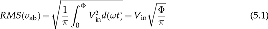
 the RMS value is determined as
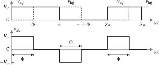
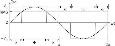
 The margin angle, α, is defined to represent half of the zero states (T0). Both Φ or α can be the modulation index for the output voltage regulation since the relation is defined as 2α + Φ = π. Therefore, the RMS value of the output voltage can also be derived as in (5.2), which is equivalent to (5.1). Thus, the output voltage can be regulated by adjusting either α or Φ.

5.1.3 Total Harmonic Distortion


 shows better representation of the ideal AC signal due to the relatively lower THD.
5.2 Sine-Triangle Modulation
5.2.1 Bipolar Pulse Width Modulation
 , where VR and VC represent the magnitudes of vr and vc, respectively. The pulse width of vab depends on the value of ma. When 0 < ma < 1, the magnitude of vab can be expected by a linear relationship with the input DC voltage:

 , where fc is the carrier frequency and fr is the modulating frequency of the reference signal. The most common frequency of fr is either 50 or 60 Hz, based on the utility grid standards. The value of mf is 11 in the demonstrated case of BPWM, as shown in Fig. 5.12. The number of pulses is counted as 11 in each fundamental cycle, which is shown as 2π in Fig. 5.12.
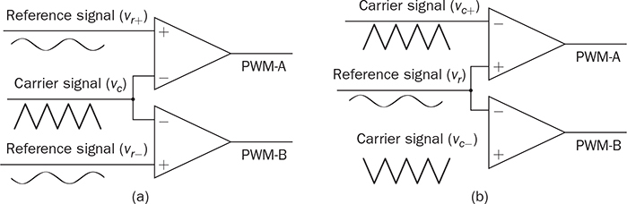
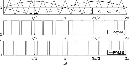
5.2.2 Unipolar Pulse Width Modulation
5.2.3 Moving Average and Filtering Circuit
5.3 Two-Switch Bridge for DC/AC
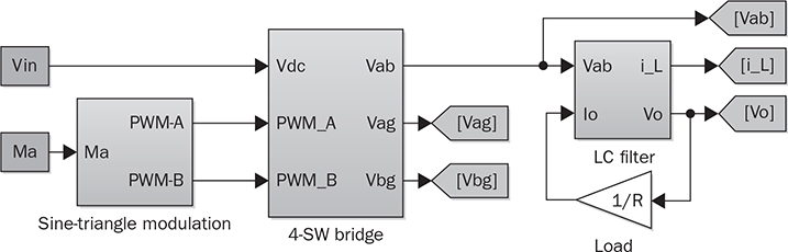
5.4 Modeling for Simulation
5.4.1 Bridge Model
5.4.2 Phase Shift Modulation
5.4.3 Bipolar Pulse Width Modulation
5.4.4 Unipolar Pulse Width Modulation
5.4.5 Integrated Modes for Simulation
5.5 Case Study
5.5.1 Chopped Square AC Output
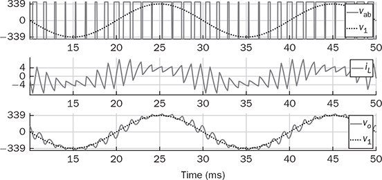
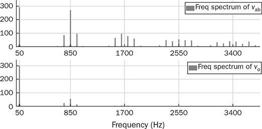
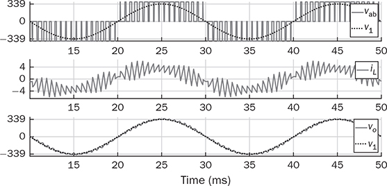
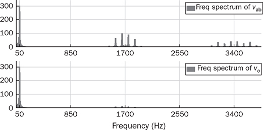
5.5.2 Sinusoidal AC Output
5.6 Summary
Bibliography
Problems