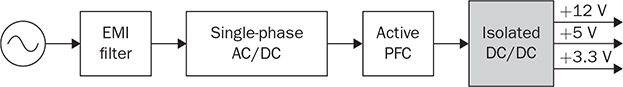
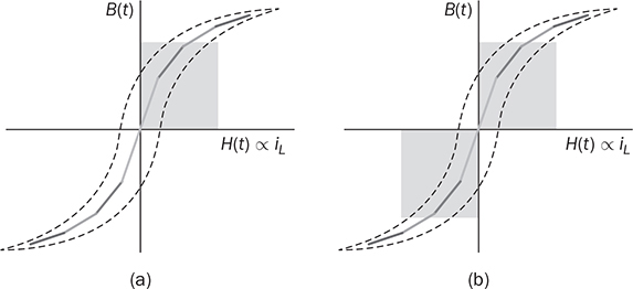
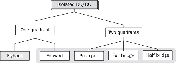
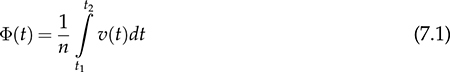
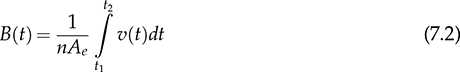
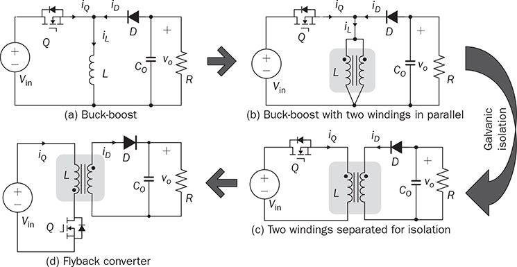
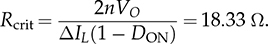
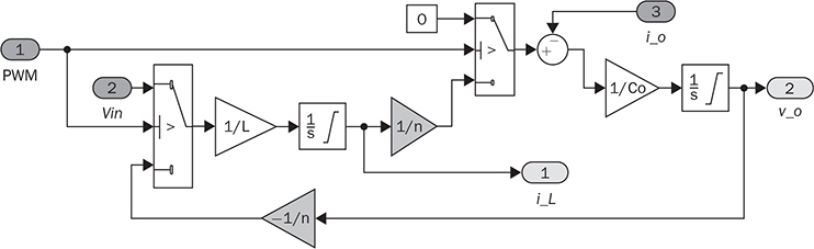
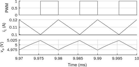
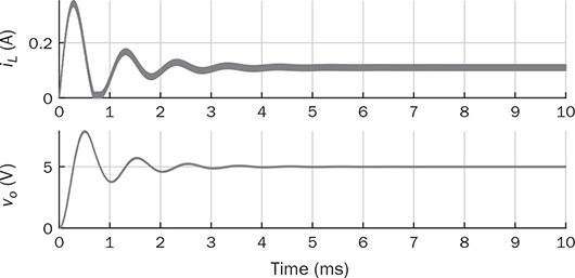
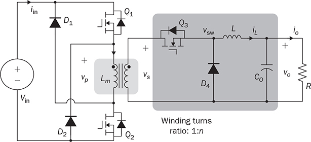
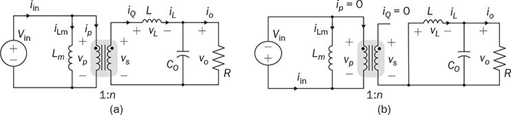
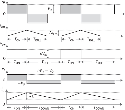
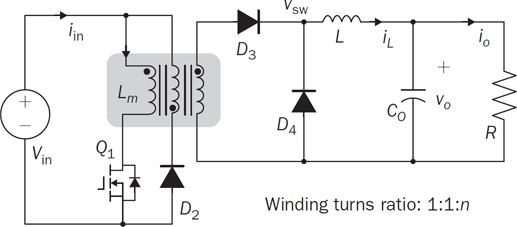
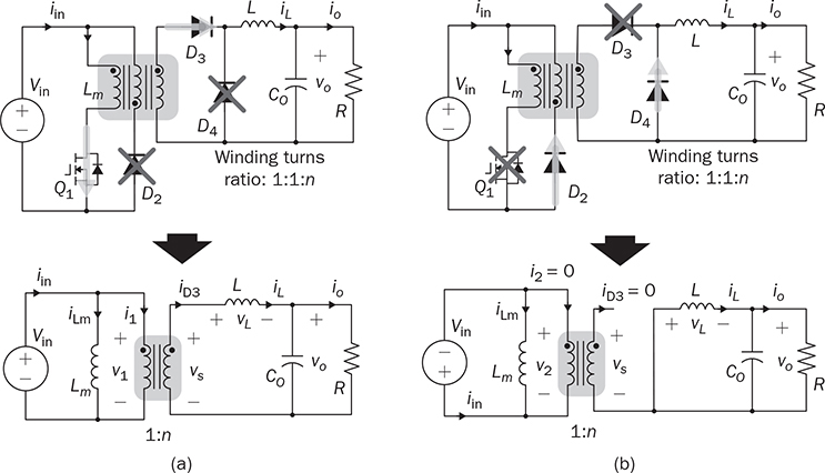
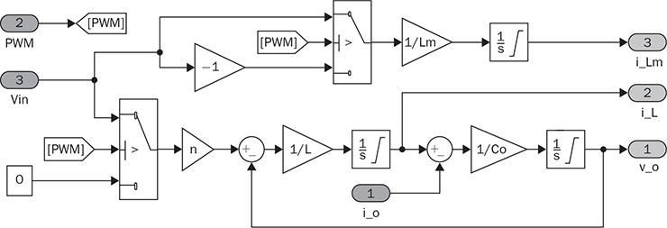
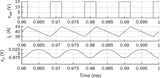
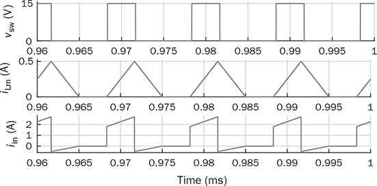
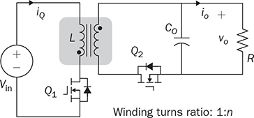
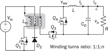
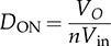
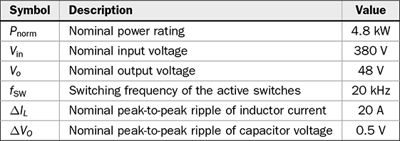
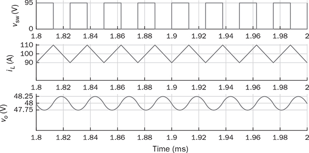
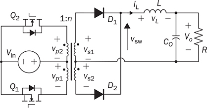
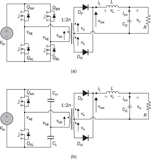
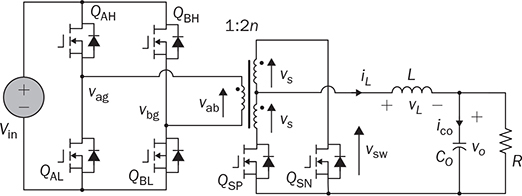
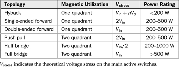
Non-isolated DC/DC topology, such as buck, boost, and buck-boost, shares the common wire connection from the input to output. For example, a buck converter, as shown in Fig. 3.7, cannot prevent high voltage from the source passing to the load in case of a short-circuit failure of the active switch. Galvanic isolated converters provide full dielectric isolation between input and output circuits. Electric codes and regulations require galvanic isolation in certain applications to improve safety and reliability. A voltage transformer can provide isolation by way of magnetic induction, which is also capable of transmitting electricity. Power transformers are classified by their operating frequencies, e.g., line frequency (LF), medium frequency (MF), and high frequency (HF). LF transformers rated for either 50 or 60 Hz are widely utilized in power networks. Modern power electronics tends to MF or HF transformers, showing the advantages of low winding turns, small size, light weight, and low cost. The HF application is the driving force to design and produce compact power supplies and converters for consumer and industry applications. Digital consumer devices have increased significantly in the past years, which should be directly powered by DC. A personal computer (PC) usually is supplied by the switching-mode power supply rated from 200 W to 1 kW. It is also termed the offline power supply. Figure 7.1 shows a typical system diagram, which represents a typical ATX power supply for desktop PCs. The device provides multiple DC outputs covering the voltage ratings of 12, 5, and 3.3 V. The important components include the electromagnetic interference filter, rectifier converting single-phase AC to DC, active power factor correction (PFC) unit, and the multiple-output DC/DC converter. The DC/DC converter shall include the function of galvanic isolation for safety purpose. The utilization of an isolation transformer can support multiple windings for different voltage levels as the outputs, as illustrated in Fig. 7.1. FIGURE 7.1 System diagram of DC power supplies for PC. The switching-mode power transformers are mainly used for HF operation, which follows the same principle and configuration byways of the multiple-windings and linkage of the magnetic field. The mode of operation makes the term differ from the conventional power transformer and creates a variety of designs and optimizations. The characteristics of a typical magnetic core is illustrated by the B-H curve discussed in Sec. 1.8. The switching operation can make the magnetic flux swings in only one quadrant based on the linearized B-H curve, as highlighted in Fig. 7.2a. Inductors commonly operate the magnetic field in one quadrant region. However, the inductive coupling can be utilized for power transformation in DC/DC conversion topologies. Same as a transformer, electrical power can pass from one winding to another through electromagnetic induction. Such utilization is often called the coupled inductor to distinguish from the standard power transformer. The inductance and energy storage capability play the important roles in applications. The topologies of flyback and forward converters are based on such this operation since the magnetic current is modulated on one polarity region, similar to the concept of inductors. The magnetic field flux density can vary up and down but maintain a unipolar direction. A classification of isolated DC/DC converters can be based on the operating region of the B-H curve, as shown in Fig. 7.3. FIGURE 7.2 B-H curves of magnetic cores of operational zone: (a) one quadrant; (b) two quadrants. FIGURE 7.3 Classification of isolated DC/DC converters. Another isolated DC/DC group includes the topologies of push-pull, full bridge, and half bridge, as shown in Fig. 7.3. The isolation transformer allows flux to swing two quadrants of the linearized B-H curve, as highlighted in Fig. 7.2b. The two-quadrant definition follows the piecewise linear approximation of the B-H curve. The magnetic current becomes AC showing the positive and negative cycles, which follow the concept of traditional power transformers. The magnetic field is considered more optimally utilized than the single-quadrant solution. The forward converter is classified in the same group as the flyback converter in terms of the operational quadrant of magnetics. It also belongs to another group of topologies called the buck-derived converters since the operational principle closely follows the nonisolated buck converters. The flyback converter is special since it is derived from the buck-boost topology. Depending on the size and design, a magnetic core can handle a certain amount of magnetic flux density. When the maximum flux density is reached, the permeability of the core significantly reduces, as illustrated in Fig. 7.2. Core saturation makes the inductors or transformers deviate from the specified inductance and lead to a magnetic current shooting in amplitude. Thus, an inductor or transformer should be adequately sized and designed to be away from the saturated magnetization. Besides the characteristics of the core material and size, the consideration also includes the applied voltage and frequency. Saturation state can be detected by monitoring the magnetizing current. The current shall increase following the predesigned inductance and the applied voltage. When a sudden increase in current is detected in steady state, the saturation happens. The magnetic flux is expressed in (7.1), which leads to the expression of the flux density in (7.2). The symbols refer to the same variables discussed in Sec. 1.8.1. When an inductor or transformer is constructed, the over-limit of B(t) results from any excessively applied “voltage × seconds.” The maximum value of the flux density, Bmax, is given in magnetic core datasheets for the design consideration to avoid saturation. Flyback converters are widely used for the low-power DC/DC conversion, which support galvanic isolation and high conversion ratio of voltage. The flyback topology is used to supply a wide range of electronic devices. The flyback converter is usually considered the simplest isolated topology that can convert the voltage from the distributed level to 5 V. Such low-power switch-mode power supplies are mainly used to supply portable electronics, e.g., cell phones and tablets. Higher capacity units are applied for the power supplies of personal computers. Recently, the flyback topology is also used in solar PV systems to step up the voltage from the low level of a single PV module to the level suitable for grid interconnection. The flyback converter is derived from the nonisolated buck-boost topology. The operation of a buck-boost converter has already been explained: energy is stored in the inductor during the on-state of the active switch; flyback operation happens when the active switch is turned off for a specific time to release the prestored magnetic energy. The inductor current naturally forces the designed circuit to release the stored energy from the magnetic field to the load. Figure 7.4 illustrates the evolution from the nonisolated converter to the flyback topology with galvanic isolation. The development from the buck-boost converter to the flyback topology can be described as follows: FIGURE 7.4 Evolution into flyback converter from buck-boost topology. • The first step is the transition from the standard buck-boost converter, as shown in Fig. 7.4a,b, by changing the single-winding inductor into a two-winding inductor. • The galvanic isolation can be added by separating the windings and creating an isolated two-winding inductor, as illustrated in Fig. 7.4c. • The final transition creates the standard form of the flyback converter, as shown in Fig. 7.4d, by manipulating the dot notation to normalize polarity and realize the low-side switch for driver and control. The winding turns ratio can also be applied to make the voltage conversion flexible. Conventional voltage transformers provide the magnetic path that instantaneously passes AC from the primary winding to others. The flyback transformer follows the same configuration that a couple of coils share a common core and transmit power from one to another. However, the operational concept is different from the function of the conventional voltage transformer. The magnetic field of the flyback transformer follows the one-quadrant operation, the same as the inductor in buck-boost topologies. Thus, it is mostly called a coupled inductor due to the short-term energy storage during the steady-state operation. Figure 7.5 shows the fundamental circuit of a flyback converter, which includes one active and one passive switch. The transformer design follows two aspects, including the winding turns ratios shown by 1:n and the magnetizing inductance, L. Figure 7.6a illustrates the equivalent circuit when Q is on-state. An amount of energy should be stored in the magnetic field via the primary winding connection with the power source. The letter L refers to the magnetizing inductance crossing the primary winding during the on-state. The value of L determines the increase in rate of the iQ. The diode is oriented to block current flow from the flyback transformer to the load side. The duration of the on-state determines the amount of energy stored. FIGURE 7.5 Circuit of flyback converter with winding turns ratio 1:n. FIGURE 7.6 Equivalent circuits of flyback converter at (a) on-state; (b) off-state. The flyback stage becomes active when Q is turned off; the equivalent circuit is shown in Fig. 7.6b. The current path through the primary winding is broken at the moment of turning off. The sudden change induces a reverse voltage of vL. The voltage appearing at the secondary winding forces the diode forward-biased. The off-state releases the pre-stored energy in L through the secondary winding and supplies to the load and charge the capacitor. In summary, the energy transferred through the flyback transformer shows an asynchronous pattern in every switching cycle, which is based on the same principle as the inductor used in buck-boost converters. The inductor current, iL, is defined to represent the current through L. The steady-state analysis of the flyback converter can be applied and based on the inductor current, iL, as shown in Fig. 7.7. In a steady state, the stored energy in L during the on-state shall be equal to the released value in the off-state of Q. The averaging value of iL becomes constant; therefore, the rising and dropping amplitudes of the inductor current is equal to the magnitude, ΔIL, as indicated in Fig. 7.7. During the on-state, the inductor current is equal to the current through Q, iQ, which can be sensed. The increasing amplitude of the inductor current is expressed by (7.3) during the on-state period, TON. Figure 7.7 shows that vL = Vin and iQ = iL. FIGURE 7.7 Steady-state waveforms of flyback converter in CCM. During the off-state of Q, the flyback transformer is disconnected from the power source. The flyback effect releases the stored power in L to the load via the secondary winding and the forward-biased diode. Following the equivalent circuit in Fig. 7.6b and the steady-state waveforms in Fig. 7.7, the dropping amplitude can be determined by (7.4) where TDOWN indicates the period that iL is decreasing. During the off-state, the inductor current cannot be directly measured but can be inferred from the measurement of the diode current since where VO is the steady-state voltage crossing the load. The steady-state condition shows that the peak-to-peak level of the inductor current ripples is constant. Combining (7.3) and (7.4) leads to the voltage conversion ratio: According to Fig. 7.7, the continuous conduction mode (CCM) can be mathematically expressed by TDOWN = TOFF and TON + TDOWN = TSW, where TSW is the period of one switching cycle. In the CCM, the voltage conversion can be expressed by where In the discontinuous conduction mode (DCM), the inductor current is saturated at the zero levels for a certain time period (TZERO) in each switching cycle during a steady state. The DCM happens when the prestored energy completely releases before the end of the off-state of Q. The zero-state shows iL = 0 and iD = 0, as shown in Fig. 7.8a, when both Q and D are off-state. The steady-state waveforms of vL, iL, and iQ are shown in Fig. 7.8b. The DCM condition is mathematically expressed by TZERO > 0, TUP + TDOWN ± TSW, or FIGURE 7.8 DCM illustration of flyback converter: (a) zero-state; (b) steady-state waveforms. The averaging value of iQ can be derived by (7.8) by following (7.7) and the waveforms shown in Fig. 7.8b. In a steady state, the power balance from the input port to the output port can be expressed by (7.9) without considering power loss. Combining (7.8) and (7.9), the voltage conversion ratio in the steady state and the DCM can be derived as shown in (7.10), where the load resistance, R, is considered. The boundary condition mode (BCM) refers to the critical condition between the CCM and the DCM. The condition is mathematically defined by (7.11). The steady-state analysis follows the same as the CCM, which shows the conversion ratio as in (7.6). The averaged value of iD can be identified by (7.12). The critical load can be derived by the equivalence of AVG(iD) ≡ AVG(io) in steady state and determined by (7.13). The operation enters the DCM when the load condition becomes R > Rcrit. A flyback converter is utilized to achieve the high step-down voltage conversion and supply 5-V DC to USB-powered loads. The design of flyback converters at the CCM can follow the following sequence: 1. Decide the winding turns ratio to make DON close to 50% with the consideration of the ratio of the input voltage and output voltage in the nominal condition. 2. Calculate on-state duty cycle and on-state time in steady state: 3. Calculate the inductance: 4. Calculate the capacitance: 5. Determine the BCM in terms of the averaged output current and the resistance. The specifications for the DC/DC stage are listed in Table 7.1. The input voltage, Vin, is referred to the nominal condition of the averaged value of vdc in the circuit schematics. Based on the specification and proposed design process, the following parameters are determined: TABLE 7.1 Specifications of Flyback Converter 1. The winding turns ratio is assigned to be n = 0.02 since the voltage conversion is from 300 to 5 V. 2. On-state duty cycle at the CCM: 3. Calculate the inductance: 4. The power rating shows that the output current IO = Pnorm/VO = 3 A; CO = 5. Critical load condition: Developing simulation model follows the schematics in Fig. 7.5 and the switching mechanism. When Q is on-state, the system dynamics can be represented in (7.14). When Q is off-state, the system dynamics can be expressed by (7.15). Based on the on/off states and the related dynamics, a Simulink model can be built, as shown in Fig. 7.9. The model follows an ideal flyback converter, which neglects power losses. The modeling is similar to the nonisolated buck-boost converter, except for the winding turns ratio and the polarity of the output voltage. The model includes three inputs, which are the pulse width modulation (PWM) command signal for the switches, the input voltage (Vin), and the output current (io). The value of io depends on the variation of load resistance (R) and the applied voltage (vo). It outputs two signals, which are the inductor current (iL) and the output voltage (vo). The saturation sign is included in the integration blocks, which constraints the inductor current (iL) and output voltage (vo) to be always positive. The implementation can support the zero-state of the DCM when iL is saturated to zero. FIGURE 7.9 Simulink model of flyback converters. Figure 7.10 demonstrates the simulated waveforms of iL and vo, which responded to the 45.45% on-state duty. The steady-state waveforms show that the averaged values of vo and iL are 5 V and 0.11 A, respectively. The simulation results agree with the converter specification in terms of the nominal output voltage and power. The load resistance is 1.67 Ω, according to the nominal operating condition. The zoom-in plots shown in Fig. 7.11 reveal the peak-to-peak ripple of iL and vo. The simulation results show that ΔIL ≈ 20 mA and ΔVO ≈ 50 mV, which is the same as specified in Table 7.1. FIGURE 7.10 Simulation results of the nominal operation (R = 1.67 Ω). FIGURE 7.11 Simulation results of the nominal operation for ripple check. When R = Rcrit = 18.33 Ω, the operation enters the critical condition of the BCM. Simulation verifies the operating condition by assigning the load resistance to Rcrit. Figure 7.12 illustrates the boundary steady state between the CCM and the DCM. When R = 37 Ω, higher than Rcrit, the operation enters the DCM. According to (7.10), the output voltage in steady state should be 7.10 V when the on-state duty of 45.45% is applied. This can be verified by the time-domain simulation, as shown in Fig. 7.13. The zero-state in each switching cycle is noticeable in the discontinuous waveform of iL. FIGURE 7.12 Simulation results of the BCM operation (R = 18.33 Ω). FIGURE 7.13 Simulation results of the DCM operation (R = 37 Ω). The forward converter shows another example of the one-quadrant operation of the B-H curve in the magnetic field. It is well-known in competition with the flyback topology. Different from the flyback topology, the on-state of the power switches in a forward converter transfers power from the source to the load. The discussion starts with the two-end-switching forward converter, in which the operational principle is easy to understand. One-end-switching, or one-transistor topology, which follows the same operational principle, will also be discussed. Figure 7.14 shows the two-end-switching forward converter. The topology applies power semiconductor switches at both ends of the primary winding. The power train circuit of the right side is the same as a nonisolated buck converter. The magnetic inductance of the transformer is shown as Lm at the primary terminal. FIGURE 7.14 Power train circuit of forward converter using multiple active switches. When all active switches are on-state, the equivalent circuit of the two-end-switching forward converter is as shown in Fig. 7.15a. All flywheel diodes are reverse-biased. The levels of iLm and iL are expected to rise due to the positive voltage crossing, as expressed in (7.16) and (7.17). The input current at the on-state is expressed as iin = iLm + ip, where ip = niL. FIGURE 7.15 Equivalent circuits when all active switches are (a) on; (b) off. where nVin = vs. The increasing amplitudes of iLm and iL depend on the on-state time, TON, which are expressed in (7.18) and (7.19), respectively. Figure 7.16 illustrates the steady-state waveform regarding the on/off operation of the switches. FIGURE 7.16 Steady-state waveform of forward converter at CCM. where VO is the averaged value of vo in steady state. When the active switches are off-state, the equivalent circuit of the two-endswitching forward converter is as shown in Fig. 7.15b. The flywheel diodes become forward-biased to flow inductor current. The equivalent circuit indicates the status of vp = −Vin, iin = −iLm, and ip = 0. The amplitudes of iLm and iL decrease due to the negative voltage crossing, as expressed in (7.20) and (7.21). The decreasing amplitudes of iLm and iL are expressed in (7.22) and (7.23), respectively. where TDOWN = TOFF = TSW − TON is the CCM of iL. In a steady state, the average current of inductors is constant. The current ripple equivalence of ΔIL in (7.19) and (7.23) leads to the conversion ratio in the steady state, which is expressed by The voltage conversion ratio at the CCM is propositional to the on-state duty, DON, in steady state and expressed by (7.25). Even though the conversion ratio is proportional to the on-state duty cycle, a constraint should be applied, which is expressed by DON ≤ 50%. Following (7.18) and (7.22), the rise and fall time of iLm in steady state can be determined as TON = TFALL. If DON > 50%, the energy stored in Lm will accumulate cycle by cycle, which can lead to saturation of the magnetic core. Thus, the CCM of iLm should be avoided in the forward converter. When n = 1, the voltage conversion ratio is the same as the nonisolated buck converter in the CCM of iL. The operation follows the same principle of the nonisolated buck converter, except for the winding turns ratio and the duty ratio limit. The two-end-switching topology requires a significant number of switches that increase the cost and loss. Further development reduces the number of power switches and simplifies the circuit design. One typical topology of forward converters is constructed by one active switch, as shown in Fig. 7.17, which is named as the one-end-switching forward converter. The magnetic reset can be achieved by the additional winding implementation and the diode, D2. The winding turns ratio is taken as 1:1:n to start the steady-state analysis. FIGURE 7.17 Forward converter constructed by one active switch with reset winding. When the active switch is on-state, the equivalent circuit is as shown in Fig. 7.18a. The input voltage is applied to cross the first winding, v1 = Vin. The diode, D3, is forward-biased due to the positive value of vs = nv1 from magnetic interconnection. Other flywheel diodes are reverse-biased. The input current at the on-state is expressed as iin = iLm + i1, where i1 = niL. The mathematical expression is the same as in (7.16)–(7.19) referring to the time period, TON, at the CCM. FIGURE 7.18 Equivalent circuit during switching: (a) on; (b) off. When Q1 is turned off, the inductor current path is created by the forward-biased diode, D2, via the second winding. The equivalent circuit is shown in Fig. 7.18b, where v2 = −Vin. The negative value is presented at the voltage terminal of vs due to the dot configuration of the transformer, which causes D3 reverse-biased. The freewheeling diode, D4, is conducting to provide a path for the inductor current, iL, which is the same operation as a buck converter. The mathematical expression is shown in (7.20)–(7.23) during the period, TDOWN. In general, the steady-state analysis shows that the one-end-switching topology follows the same mathematical expressions as the analysis for the two-end-switching forward converter if the winding turns ratio is compatibly applied. Thus, the voltage conversion ratio for the one-end-switching topology is the same as the expressions in (7.24) and (7.25) for the CCM. The switching duty ratio is also constrained to ensure enough off-time to reset the magnetic current in each switching cycle. It should be noted that the maximum limit of DON can be changed from 50% if the winding turns ratio is adjusted to be different from the 1:1:n setting. The additional winding configuration can make the resetting of the magnetic current, iLm, faster or slower, which is different from the operation of the two-end-switching topology. The CCM of the forward converter refers to the continuity of the inductor current at the output side, which follows the same circuit as the buck converter. The design should include the transformer specification in terms of the winding turns ratio and the magnetizing inductance. The constraint should be applied to ensure enough off-state time to reset the magnetic current in each switching cycle. According to the rating at the CCM and the nominal operating condition, the following sequence can be followed: 1. Determine the winding turns ratio according to the ratio of the input voltage and output voltage and the constraint of DON. 2. Calculate the on-state duty cycle and time in steady state: 3. Calculate the inductance: 4. Calculate the capacitance of CO following (3.15) for a buck converter. 5. Determine the critical load condition in terms of the averaged output current and the resistance. The magnetizing inductance can be derived or measured when the transformer is designed to meet the conversion ratio and power rating. The case study follows the specifications listed in Table 7.2. The single-transistor forward converter, as shown in Fig. 7.17, is selected to achieve the high step-down voltage conversion and supply steady 5-V load. Based on the specification and proposed design process, the following parameters can be derived: TABLE 7.2 Specifications of Forward Converter 1. The winding turns ratios are assigned to be 1:1:n and n = 0.05 due to the conversion ratio requirement of 5/300 and the upper limit of DON. 2. On-state duty cycle at CCM: 3. Calculate the inductance: 4. Calculate the capacitor: 5. Critical load condition: When the DCM is considered for iL, the voltage conversion does not follow the same ratio as in (7.25). Following the DCM analysis of a buck converter, the on-state time of the forward converter in each switching cycle can be determined by where VO is the specified voltage of the output in steady state. The on-state duty cycle is expressed by (7.27) to regulate the converter for the desired output. Based on the on/off switching operation, a Simulink model can be built to simulate the switching operation of forward converters. Figure 7.19 demonstrates the model configuration including the output signals of iLm, iL, and vo. The model includes three inputs, which are the pulse width modulation (PWM) command signal for the switches, the input voltage (Vin), and the output current (io). The value of io depends on the instantaneous voltage of vo and load condition. Two single-pole-double-throw (SPDT) switches are utilized in the Simulink model for switching between the dynamics among the onstate and the off-state. The winding turns ratio is shown in the model to represent the transformer. Following (7.16) and (7.18), the inductor current, iLm, can be revealed by simulation. The rest of the modeling is similar to the nonisolated buck converter, except for the additional consideration of the winding turns ratio and the magnetic inductance. The saturation sign is shown in the Simulink blocks for integration, which constraints the levels of iL, vo, and iLm to be positive when the diodes are implemented. FIGURE 7.19 Simulink model of the power train circuit of forward converters. Following the case study in Sec. 7.3.3, the forward converter is simulated to prove the design. Figure 7.20 demonstrates the simulated waveforms of iL and vo. When the 33% on-state duty cycle is applied, the averaged values of vo and iL in the steady state are 5 V and 40 A, agreeing with the converter specification in terms of the nominal output voltage and power. The peak-to-peak ripples also follow the specified values, which verify the designed parameters. The waveforms of iin and iLm are illustrated in Fig. 7.21. In the case study, the magnetizing inductance of the transformer is assigned to be 2 m. The current peak of iLm is 0.5 A, which agrees with (7.18). Since DON < 50%, the magnetic current, iLm, is reset to zero in every switching cycle. FIGURE 7.20 Steady-state waveforms of vsw, iL, and vo at the nominal condition. FIGURE 7.21 Steady-state waveforms of vsw, iLm, and iin at the nominal condition. Flyback and forward topologies mainly focus on low-power applications. The conventional topologies include diodes in the circuits, as shown in Figs. 7.5 and 7.17. Dealing with ELV applications, the voltage drop of diodes weighs high in loss that hinders conversion efficiency. The latest configuration adopts more and more synchronous rectifications, which replace the diodes at the low voltage side with field effect transistors (FETs). Figure 7.22 illustrates the synchronous switching implementation for a flyback converter, which applies one metal-oxide semiconductor field-effect transistor (MOSFET) to replace the diode at the secondary side. The on-state of Q2 is synchronous with the antiparallel diode to conduct during the flyback state in each switching cycle. The conversion efficiency can be significantly improved if the output voltage rating is less than 12 V. FIGURE 7.22 Flyback converter with synchronous rectifier. Figure 7.23 shows the synchronous switching implementation for the forward topologies. The diode D2 remains in the circuit since its conduction loss does not weigh high in the distribution when Vin > 100 V. The conduction loss of the MOSFETs, Q3 and Q4, is expected to be low in comparison to the diode implementation for ELV applications. FIGURE 7.23 Synchronous switching solution for forward converter. An isolated DC/DC topology is called the full-bridge isolated DC/DC converter, as shown in Fig. 7.24a. Different from the forward converter, the isolation transformer directly passes AC from one terminal to another. The term “full bridge” refers to the utilization of the active four-switch bridge for the DC/AC conversion, and the passive four-switch bridge for the AC/DC conversion. Even though the circuitry is more complicated than the topologies introduced earlier, the converter follows a simple design concept, as demonstrated in Fig. 7.24b. Power passes from the source to the load via the path of DC/AC, AC/AC, AC/DC, and filtering. The voltage transformer naturally performs the AC/AC voltage conversion from one winding to others. The magnetic flux density in the transformer swings two quadrants of its B-H curve, as illustrated in Fig. 7.24b. FIGURE 7.24 Full-bridge isolated DC/DC converter: (a) schematics; (b) concept illustration of power flow. The DC/AC stage can be modulated and controlled to output the desired pulse width and frequency of AC, as discussed in Chap. 5. The diode bridge is a full-wave rectifier that has been discussed and analyzed in Chap. 6. The key components also include the isolation transformer and the LC circuit for low-pass filtering. The active four-switch bridge can produce the AC signal, vab, in high frequency. It is an effective way to minimize the size and cost of the isolation transformer. The high switching frequency also appears at the DC signal, vsw, which lowers the size of L and CO. For the four-switch active bridge, the complication of sine-triangle modulation is unnecessary since the power quality of the interlinking AC is not a concern. The modulation should produce chopped-square waveforms in vab to represent the amplitude and frequency of AC. As discussed in Sec. 5.1, the phase-shift technique can produce the desired pulse width through the modulation process. Figure 7.25 illustrates the key waveforms of the converter in the CCM and steady state. The pulse width of vab appears the same as that in the waveforms of vs and vsw. The AC signals pass the transformer, which is expressed by vs = nvab corresponding to the winding turns ratio. The signal of vs is rectified into DC as vsw. From the point of vsw, the operation follows the same principle as the nonisolated buck converter regarding the steady-state analysis. Figure 7.26 illustrates the equivalent circuit of the output stage of the isolated converter. The duty ratio of vsw determines the averaged value of the output voltage and current. FIGURE 7.25 Steady-state waveforms of isolated buck converter. FIGURE 7.26 Equivalent circuit of the output stage of full-bridge isolated converter. Following the waveforms in Fig. 7.25, the voltage conversion ratio in steady state can be derived as in (7.28). The voltage conversion ratio becomes as in (7.29) since TON + TDOWN = TSW in CCM. The duty ratio, DON, refers to the signal of vsw expressed The modulation is performed by the active four-switch bridge at the DC/AC stage. According to the phase-shift modulation in Sec. 5.1.2, the phase delay angle, Φ, is the control variable to determine the pulse width of vab, vs, and vsw. The relation between Φ and DON is proportional and expressed in (7.30). Therefore, the output voltage of the full-bridge isolated DC/DC converter can be determined by the applied phase angle, Φ, as shown in (7.31). where VO represents the averaged value of the output voltage. It should be noted that the switching frequency of the DC/AC stage is expressed by Following the equivalent circuit in Fig. 7.26, the diode bridge serves as the freewheeling purpose of the inductor current, iL. Thus, the discontinuous conduction mode (DCM) results when the inductor current, iL, is saturated to zero for a certain time during the periodic cycle in steady state. The output voltage cannot be predicted by the CCM in (7.31). However, the steady-state analysis for the DCM can follow the same procedure for the nonisolated buck converter and refers to the equivalent circuit in Fig. 7.26. The design of the full-bridge isolated DC/DC converter is mainly based on the CCM operation. The value of fsw is referred to as the switching frequency of the active swtiches. According to the nominal operating condition, the following procedure can be followed for design: 1. Determine the winding turns ratio of the isolation transformer according to the ratio of the input voltage and output voltage and the constraint of DON and Φ. 2. Calculate on-state duty cycle and on-state time at steady state: 3. Calculate the inductance: 4. Calculate the capacitance of CO following the same procedure as in (3.15) for the buck converter. 5. Determine the critical load condition in terms of the averaged output current and the resistance. Following the circuit in Fig. 7.24, the specifications for a case study are shown in Table 7.3. Thus, the converter can be designed step by step. TABLE 7.3 Specifications of Forward Converter 1. The winding turns ratio is assigned to be n = 0.25, following the nominal conversion ratio of 48/380 and the upper limit of DON. 2. On-state duty cycle at the CCM: 3. Calculate the inductance: 4. Calculate the capacitor: 5. BCM: Based on the previous discussion for DC/AC, AC/DC, and buck converters, the simulation model for the full-bridge isolated DC/DC conversion can be built by integrating the individual functional blocks, as shown in Fig. 7.27. The DC/AC block follows the same development described in Sec. 5.4.1, as shown in Fig. 5.23. The functional block of phase-shift modulation has been developed and shown in Fig. 5.24. The operations of the ideal transformer and the AC/DC conversion are simplified by the mathematical computation of scaling and absolution, respectively. The model takes the inputs of the phase-shift angle, Φ, and the input voltage, Vin. It outputs the variables of vag, vbg, vab, vs, vsw, iL, and vo for analysis. For variables, refer to the circuit diagram in Fig. 7.24. FIGURE 7.27 Simulation model for full-bridge isolated DC/DC. Figure 7.28 demonstrates the simulated waveforms regarding the voltage signals of vag, vbg, vab, and vs, responding to the phase-shift angle Φ = 1.59 rad, or 90.95°. The phase shift between vag and vbg produces the waveform of vab, which is the modified square wave of 20 kHz. The voltage is transformed to vs through the voltage transformer, where the winding turns ratio is applied. Figure 7.29 illustrates the simulated results of vsw, iL, and vo. The steady-state waveform shows that the averaged values of vo and iL are 48 V and 100 A, respectively, agreeing with the converter specification in terms of the nominal output voltage and power. The peak-to-peak ripples of the current and voltage also follow the specified values, 20 A and 0.5 V. The periodic cycle of the DC signals in vsw, iL, and vo is half of that of the AC signals of vab and vs. The ripple frequency of vsw refers to 40 kH, which is two times higher than the switching frequency of the active switches. FIGURE 7.28 Simulated waveforms of vag, vbg, vab, and vs. FIGURE 7.29 Simulated waveforms of vsw, iL, and vo. A push-pull converter is an isolated DC/DC topology that follows the same conversion sequence shown in Fig. 7.24b. The typical configuration of a push-pull conversion is shown in Fig. 7.30, including two active switches and two passive switches. One distinct feature lies in the relatively lower component count in comparison with the full-bridge solution. The topology takes the advantage of the transformer utilization, where both the primary and secondary windings are center-tapped to distinguish the AC polarity. FIGURE 7.30 Circuit of push-pull isolated DC/DC converter. Both active switches are located at the low side to simplify the gate driver design. Q1 and Q2 are controlled to conduct alternatively with identical lengths of time. When Q1 is turned on for conduction, the input voltage is applied: vp1 = Vin, as shown in Fig. 7.31. Based on the winding configuration indicated by the dot convention, the secondary voltages of the transformer follow vs1 = vs2 = nvp1. The voltage potential of vs1 makes D1 forward-biased to conducting current; meanwhile, D2 is reverse-biased. When Q2 is turned on, the input voltage is applied: vp2 = −Vin. The secondary voltages of the transformer follow vs1 = vs2 = nvp2. The negative value of vs2 makes D2 forward-biased for current conduction. Meanwhile, D1 is reverse-biased due to the winding configuration indicated by the dot convention. When both Q1 and Q2 are turned off, the voltage level of the primary side becomes zero. During the off-state, the freewheeling function of iL makes the diode forward-biased for conduction via the winding. The amplitude of iL will drop to a certain level. In the CCM, the voltage conversion ratio at the steady state is expressed by FIGURE 7.31 Waveforms produced by push-pull DC/DC converter. where DON = TON/TSW, as shown in Fig. 7.31. Following the operational principle, the Simulink model for the push-pull converter can be constructed, as shown in Fig. 7.32. The switching operation produces the voltage signals of vp1 and vp2. The model output is the switching-node voltage, vsw. The LCR circuit can be built by following the same Simulink model as the nonisolated buck converter when vsw is applied. Special attention is given so that the frequency of vsw is not referred to the same as the switching frequency of the active switches Q1 and Q2. FIGURE 7.32 Simulink model for push-pull converter. The center-tapped configuration of the isolation transformer is used in the push-pull converter, which reduces the component count. The same configuration can be applied for the full-bridge and half-bridge isolated DC/DC converters to simplify the AC/DC conversion. Figure 7.33 illustrates the circuit of the rectifier which is formed by two diodes instead of four. When the winding turns ratio is configured accordingly, the converter follows the same principle as the four-diode bridge for the AC/DC conversion. This implementation is also beneficial to reduce the diode conduction loss by half. The circuit of the half-bridge solution is different from the full-bridge isolated converter since two series-connected capacitors replace the active switches and form Leg B, as shown in Fig. 5.3b. Such DC to single-phase AC conversion has been introduced in Sec. 5.3 when the two-switch bridge is used. FIGURE 7.33 Center-tapped configuration of transformer for (a) full bridge; (b) half bridge. For ELV applications, the diode configuration weights high in power losses. Thus, the isolated DC/DC converter adopts more and more synchronous rectifications to achieve high conversion efficiency. On the secondary side, the rectification can be achieved by two FETs, as shown in Fig. 7.34. The on-state of QSP creates a path for the positive half cycle. On the other hand, the on-state of QSN inverts the negative half cycle into DC. The FETs are laid out at the low side for simple gate driving circuits. The active switches are turned on or off following the same conduction pattern as in diodes for the AC/DC conversion. FIGURE 7.34 Full-bridge isolated converter with implementation of center-tapped transformer and synchronous rectifier. Galvanic isolation is required by power system regulation for safety and reliability. Figure 7.3 gives the classification of the galvanic-isolated DC/DC converters based on the utilization of the magnetic field and high-frequency switching. One group, including flyback and forward converters, operates the magnetic flux to swing one quadrant regarding the linearized B-H curves. The others follow the two-quadrant operation of B-H curves through the isolation transformer. The converters include the topologies of push-pull, half bridge, and full bridge. The flyback topology is evolved from the nonisolated version, buck-boost converter. Energy is stored into the magnetic field through the primary side connection with the power source. The flyback phenomena allow the stored energy to be dumped to the load side through the flyback transformer in a discrete time. It should be noted that the flyback transformer is the same as the coupled inductor but supports galvanic isolation. The time split is regulated by the on/off time of the main switch. Thus, the capability of energy storage is critical for the flyback transformer design since it follows the operation of an inductor. Analysis, simulation, and design can mostly follow the same as the buck-boost with the consideration of CCM and DCM. Thanks to the simplicity and galvanic isolation, flyback converters are widely available for low-power applications, such as USB chargers and computer power supplies. The interleaving approach or parallel configuration can boost the power capacity. The DCM operation of a flyback converter supports zero current switching, which is sometimes preferably applied in specific applications. A big family of isolated DC/DC converters follows the design concept of the nonisolated buck topologies, which include the forward, full bridge, half bridge, and push-pull converters. Forward topology is commonly considered the isolated version of buck converters since it strictly follows the same operational principle. When the winding turns ratio is reset to 1, the voltage conversion ratio becomes the same as the buck converter in the CCM. A forward converter passes energy from the primary to the secondary during the on-state of the main switch. When the switch is turned off, the magnetic current needs to go through the freewheeling operation via dedicated channels. At the point of the magnetic field, the forward transformer is the same as the coupled inductor but supports galvanic isolation. The rest of the topologies, e.g., full bridge, half bridge, and push-pull, simply take the concept of conventional isolation transformers but operate at high frequency. Table 7.4 shows a quick guide to select isolated DC/DC converters. The choice is based on the converter circuit complexity and power rating. The full-bridge formation is considered as the most complete solution for targeting high-power utilizations. Others can be adopted for the middle range of the power rating. The variety of the isolated DC/DC converters is also available to minimize either the usage of power semiconductors or conduction loss caused by the forward voltage drop of diodes. The winding configuration can also minimize the usage of power semiconductors. TABLE 7.4 Summary of the Isolated DC/DC Converters 1. D. W. Hart, Power electronics, McGraw-Hill, 2011. 2. W. Xiao, Photovoltaic power systems: modeling, design, and control, 1st ed., Wiley, 2017. 3. R. W. Erickson and D. W. Maksimovic, Fundamentals of power electronics, 2nd ed., Springer, 2007. 7.1 Follow the simulation modeling process to build your own models for the flyback, forward, and full-bridge DC/DC converters. Use the examples in this chapter to verify the model accuracy and limit. 7.2 A flyback DC/DC converter is shown in Fig. 7.5. The input voltage (Vin) is sourced from a 48-V rated battery, but the voltage changes between 48 to 54 V depending on the state of charge. The amplitude of the output voltage should be constantly maintained at 380 V for DC loads. The nominal load resistance is Rnorm = 722 Ω; the switching frequency is fsw = 100 kHz. The peak-to-peak value of the inductor current ripple at steady state is specified to be lower than ΔIL = 1 A. The peak-topeak ripple of the output voltage is specified to be lower than ΔVO = 1.9 V. (a) Design the winding turns ratio for the flyback transformer. (b) Based on the CCM, determine the on-state duty ratio of PWM for the input voltage of 48 and 54 V, separately. (c) Based on the CCM, with consideration of the input voltage variation, determine the proper value of the inductance L and the output capacitance CO to meet the specification. (d) When Vin = 50 V and there is a nominal duty ratio for 380 V output, compute the critical value of the load resistance, Rcrit, which is the boundary between the CCM and DCM. (e) When the load resistance is 10 kΩ and Vin = 54 V, and the on-state duty cycle of PWM is 50%, verify the analysis by simulation. 7.3 The forward topology, as shown in Fig. 7.17, is required to make the conversion from a 30-V PV generator to the 380-V DC bus. The power rating is 240 W. The switching frequency is fsw = 100 kHz. (a) Specify the winding turns ratio for the transformer design. (b) Based on the CCM, determine the on-state duty ratio of PWM for the nominal operation; compute the on-state time, TON, and off-state time, TDOWN. (c) If the magnetic inductance is Lm = 30 μH, determine the falling time period of the current, iLm; determine the peak-to-peak value of iLm. (d) When the peak-to-peak value of the inductor current ripple at steady state is specified to be lower than ΔIL = 0.3 A, compute the required inductance, L, at the output side. (e) When the peak-to-peak ripple of the output voltage is specified to be ΔVO = 1 V, compute the required capacitance, CO, at the output side. (f) Simulate the circuit based on the nominal condition to demonstrate the waveforms of vo, iL, iLm, and iin. 7.4 A full-bridge isolated DC/DC converter should be designed for the nominal conversion from 380 to 12 V. The power rating is 2.4 kW. The power train circuit is shown in Fig. 7.34. The switching frequency of the active switches is 20 kHz. The modulation is based on the phase-shift technology. The peak-to-peak value of the inductor current ripple at steady state is specified to be lower than ΔIL = 40 A. The peak-to-peak ripple of the output voltage is specified to be lower than ΔVO = 0.2 V. (a) Design the winding turns ratio for the isolation transformer. (b) Based on the CCM, determine the on-state duty ratio of the signal, vsw; the on-state time, TON; the off-state time, TDOWN; and the phase-shift angle, Φ. (c) Based on the CCM, determine the proper value of the inductance, L, and the output capacitance, CO, to meet the specification. (d) Compute the critical value of the load resistance, Rcrit, which is the boundary between the CCM and DCM. (e) Simulate the converter operation at the nominal load condition. 7.5 A half-bridge isolated DC/DC converter should be designed for the nominal conversion from 380 to 12 V. The power rating is 2.4 kW. The switching frequency of the active switches is 20 kHz. The peak-to-peak value of the inductor current ripple at steady state is specified to be lower than ΔIL = 40 A. The peak-to-peak ripple of the output voltage is specified to be lower than ΔVO = 0.2 V. (a) Design the winding turns ratio for the isolation transformer. (b) Based on the CCM, determine the on-state duty ratio of the signal, vsw; the on-state time, TON; the off-state time, TDOWN; and the duty ratio for each active switch. (c) Based on the CCM, determine the proper value of the inductance, L, and the output capacitance, CO, to meet the specification. (d) Compute the critical value of the load resistance, Rcrit, which is the boundary between the CCM and DCM. (e) Simulate the converter operation at the nominal load condition. (f) Comment on the difference from the full-bridge solution in terms of design. 7.6 A push-pull isolated DC/DC converter should be designed for the nominal conversion from 380 to 12 V. The power rating is 480 W. The power train circuit is shown in Fig. 7.30. The switching frequency of the active switches is 50 kHz. The peak-to-peak value of the inductor current ripple at steady state is specified to be lower than ΔIL = 20 A. The peak-to-peak ripple of the output voltage is specified to be lower than ΔVO = 0.2 V. (a) Design the winding turns ratio for the isolation transformer. (b) Based on the CCM, determine the on-state duty ratio of the signal, vsw; the on-state time, TON; the off-state time, TDOWN; and the duty ratio for each active switch. (c) Based on the CCM, determine the proper value of the inductance, L, and the output capacitance, CO, to meet the specification. (d) Compute the critical value of the load resistance, Rcrit, which is the boundary between the CCM and DCM. (e) Simulate the converter operation at the nominal and critical load conditions.
CHAPTER 7

Isolated DC/DC Conversion
7.1 Region of Magnetic Field
7.1.1 Operational Quadrant and Classification
7.1.2 Critical Checkpoint for Saturation
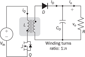
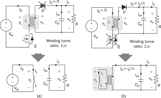
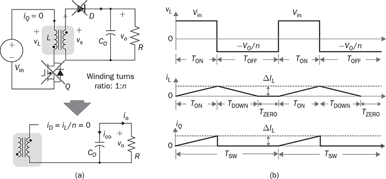
7.2 Flyback Topology
7.2.1 Derivation from Buck-Boost Converter
7.2.2 Flyback Operation
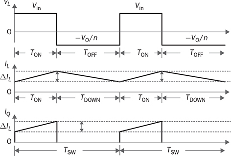
7.2.3 Continuous Conduction Mode

 and
and  .
.


 and DOFF = − DON.
7.2.4 Discontinuous Conduction Mode
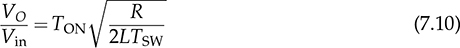
 . The voltage conversion ratio at DCM follows the same derivation from (7.3) into (7.5). However, TDOWN cannot be directly determined by the difference between TSW and TON due to the unknown value of TZERO. In the DCM, TON is the control variable and is known for the following analysis. The ripple current of iL can be determined by


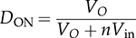
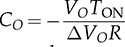
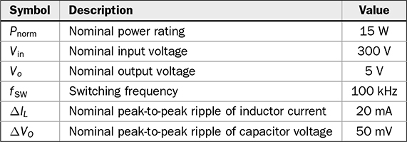
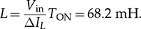
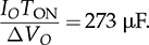
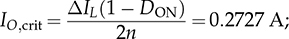
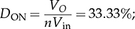
7.2.5 Circuit Specification and Design
 and
and 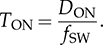 .
.
 derived by (7.3).
 or
or 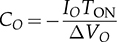 derived from the amplitude of the voltage drop at the on-state.
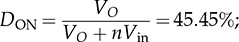
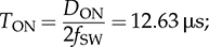
 4.545 μs.
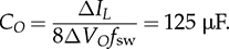
 .
.
 .
.
7.2.6 Simulation for Concept Proof


7.3 Forward Converter
7.3.1 Two-End-Switching Topology


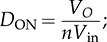
7.3.2 One-Transistor Solution
7.3.3 Circuit Specification and Design
 TON =
TON = 
 TDOWN derived from (7.23).
 TDOWN = 6.67 μs.


7.3.4 Simulation for Concept Proof
7.4 Synchronous Rectification
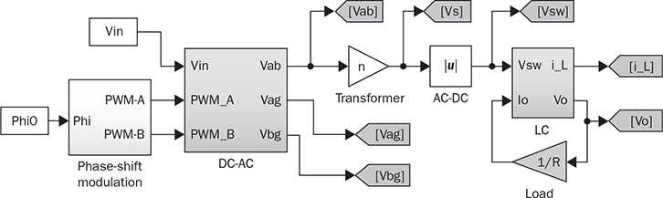
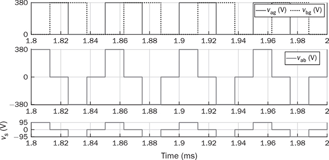
7.5 Full Bridge for DC/AC Stage
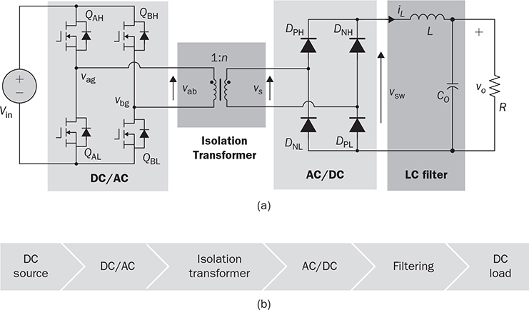
7.5.1 Steady-State Analysis
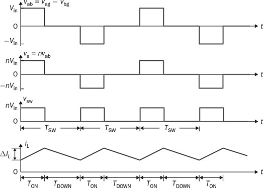
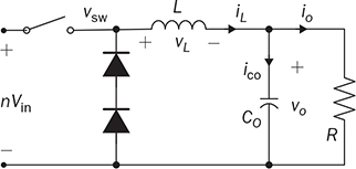


 , as shown in the waveform of vab in Fig. 7.25. The difference is caused by the rectification from the single-phase AC to DC.
7.5.2 Circuit Specification and Design
 , TDOWN = 1 − TON, and Φ = DONπ.
 TDOWN following the same measure for the nonisolated buck converter.

 TDOWN = 12.37 μs; Φ = 1.59.
 TDOWN = 29.68 μH.

7.5.3 Simulation for Concept Proof
7.6 Push-Pull Converters

7.7 Variation and Enhancement
7.8 Summary
Bibliography
Problems